| Posted: Jan 23, 2014 |
Active microfluidic chips inkjet-printed on normal paper |
| (Nanowerk Spotlight) Paper has emerged as a focus area for researchers developing innovative techniques for printed basic electronics components. Electronic paper displays are already a commercial reality and prototypes of things like foldable paper-based batteries, paper solar cells, and paper-based metamaterial biosensor are under development. |
| Another area where paper could lead to low-cost innovative devices and applications is lab-on-a-chip technology. Currently, these microfluidic devices are fairly expensive due to their lithography-based fabrication process with channels patterned in glass or plastic and tiny pumps and valves directing the flow of fluids. |
| Inexpensive paper-based sensing kits already play an important role in ready-to-use diagnostics. Researchers have even managed to create an inexpensive microfluidic platform on hydrophobic paper with laser treatments (see "New lab-on-chip advance uses low-cost, disposable paper strips"). |
| In new work, researchers in Korea have now, for the first time, used paper as a platform material for actively actuating an electronic microfluidic chip. This novel, powered fluidic chip – known as an active paper open chip (APOC) – allows the full range of fluidic operations by implementing an electric input on paper via an electrowetting technique. |
| "Instead of using the passive capillary force on the pulp in the paper to actuate a continuous flow of a liquid sample, we used inkjet printed electrodes to transport a single, discrete drop or a group of digital liquid drops perfectly along programmed trajectories," Kwanwoo Shin, a professor in the Department of Chemistry and Institute of Biological Interfaces at Sogang University who leads the Biological Interface Laboratory, tells Nanowerk. "The patterned electrodes, which we designed on a desktop computer, were printed on normal paper with conductive carbon nanotube ink by using a regular office inkjet printer." |
| The team reported their findings in the January 13, 2014 online edition of Advanced Materials ("Active Digital Microfluidic Paper Chips with Inkjet-Printed Patterned Electrodes"). |
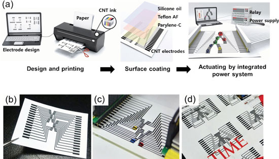 |
| a) Overview of the fabrication process for an active microfluidic paper chip: design using a personal computer and inkjet-printing of the patterned electrodes; coating with dielectric and oil films; actuation of reagent drops on the paper chip by using an integrated switching power system. b) Photograph of the printed paper chip; c) photograph of a microfluidic paper chip assembled in the integrated switching power system; and d) photograph of the patterned electrodes on Time magazine paper to show their potential use with a cheap and ubiquitous recycled material. (Reprinted with permission from Wiley-VCH Verlag) |
| "The most noticeable difference between active and passive paper-based microfluidic devices is the existence of a patterned array of electrodes on the paper such that the capillary force on the substrate’s surface can be actively tuned with an external voltage," explains Shin. "The basic principle of actuating drops on paper is the use of an electric field to adjust the electrowetting-induced surface tension between a drop and a counter-electrode beneath the surface." |
| This active paper chip has many advantages largely due to paper itself being a low-cost, flexible, printable, hydrophilic and easily disposable material. |
| Shin points out that this active paper-based microfluidic chip is the first device that fuses two new emerging microfluidic devices: the passive microfluidic paper-based analytical device (m-PAD) and the active plastic- and glass-based lab-on-a chip (LoC). |
| "For many years, we have realized that water drops can be transported by sequential electrowetting, which was only possible on micropatterned metallic electrodes," he recounts the background to this work. "A couple of years ago, a team at the Institute of Biological Interfaces at Sogang University (Prof. Kwanwoo Shin and Prof. Oh-Sun Kwon) developed a carbon-nanotube based inkjet printing method, allowing us to produce highly conducting CNT patterns on paper. Then, together with a group from Chungnam National University (Prof. Jae-Hak Choi) and Advanced Radiation Technology Institute (Mr. C.-H. Jung), we accordingly proved that the inkjet-printed patterned electrodes can be employed to actuate liquid drops on paper, not only photo paper, but virtually any paper, like recycled magazine paper, or photo-copy white paper." |
| One of the problems the team had to overcome was related to the printing resolution. Because they used the printed pattern of home-made CNT-ink, the printing resolution initially couldn't be reduced to less than 50 µm, which definitely limited the minimization of the gap size between electrodes. They resolve this obstacle with two ideas – coating the surface with silicon oil, and using alternative current (AC) voltage instead of direct current (DC) voltage to increase the drop distance. |
| Shin is confident that, as the related technologies – i.e. ink-jet printing and conducting ink formulation – are improving, the printing resolution can be minimized further to reduce the cost of chip fabrication. |
| The key advantage in fabricating APOCs is that electrode patterns can be designed and printed on paper quickly, finely and precisely without complicated wet-lab processes. A printing method could become the simplest all-in-one method for designing and fabricating such microfluidic chips, thereby replacing complex, multi-step conventional optical lithography and enabling chip production at the point of care, particularly in remote and isolated regions with limited resources. |
| To demonstrate the simplicity of this production process, the researchers used inkjet printing with a commercial home/office inkjet printer and fabricated electrodes on commercially-available photo paper by using a homemade conductive carbon nanotube ink (which the team described in a previous paper: "Fabrication and characterization of inkjet-printed carbon nanotube electrode patterns on paper"). |
| In order to demonstrate the potential use as truly point-of care application, the researchers are planning to demonstrate the real-time, on-site production of enzyme-linked immunosorbent assay kits (ELISA) in Cambodia via remotely designed devices, simplifying the workflow and improving the reaction accuracy tremendously in the laboratory compared to conventional methods. |
| "In a year or so, we will show versatile paper-based ELISA diagnosis kits, which are applicable, at least, to 10-the most fatal diseases in Africa, including HIV, and Malaria," says Shin. |
| "It is worth mentioning the possibility of combining the two types of chips – passive and active – in a so-called hybrid paper chip," he continues. "We expect that this new next generation device should attract a lot of interest in developing a wide range of functionalities on paper chips. Some potential applications are: a chip having complementary control flow rate of a drop and a flow of sample solution; passive cellulose paper providing filtering out any impurities of particles resolved in sample solution; and three-dimensional chips composed of sandwiched layers." |
 By
Michael
Berger
– Michael is author of four books by the Royal Society of Chemistry:
Nano-Society: Pushing the Boundaries of Technology (2009),
Nanotechnology: The Future is Tiny (2016),
Nanoengineering: The Skills and Tools Making Technology Invisible (2019), and
Waste not! How Nanotechnologies Can Increase Efficiencies Throughout Society (2025)
Copyright ©
Nanowerk LLC
By
Michael
Berger
– Michael is author of four books by the Royal Society of Chemistry:
Nano-Society: Pushing the Boundaries of Technology (2009),
Nanotechnology: The Future is Tiny (2016),
Nanoengineering: The Skills and Tools Making Technology Invisible (2019), and
Waste not! How Nanotechnologies Can Increase Efficiencies Throughout Society (2025)
Copyright ©
Nanowerk LLC
|

Become a Spotlight guest author! Join our large and growing group of guest contributors. Have you just published a scientific paper or have other exciting developments to share with the nanotechnology community? Here is how to publish on nanowerk.com. |
