| Posted: Feb 06, 2014 |
Integrated optical and AFM metrology (page 1 of 2) |
| (Nanowerk Application Note) Surface metrology and characterization is ever more critical for overall product performance in wide ranging applications across the semi-conductor, LED, data storage, medical and automotive industries. 3D optical microscopes are among the fastest and most accurate imaging systems on the market today, and are employed in these industries for rapid and precise process monitoring, product development, and research. However, there are instances where they have performance limitations and the benefits of scanning probe/atomic force microscopy provide a clear advantage. |
| A few examples include thin film metrology applications that require very high lateral resolution, such as defect review, that require a contact method to mitigate dissimilar materials offsets. To address such applications, Bruker has introduced an atomic force microscope (AFM) module that mounts directly to a 3D optical microscope to provide unprecedented flexibility for surface metrology. This application note provides an overview of basic system operation and an application example for the NanoLens™ AFM on a ContourGT 3D optical microscope. |
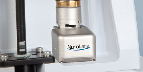 |
| Figure 1: NanoLens AFM Module installed on a bench-top ContourGT-I 3D Optical Microscope. |
| NanoLens AFM |
| The NanoLens AFM consists of an electronics control box and an AFM scan head that can be mounted to a Bruker 3D optical microscope turret or single objective adapter. The electronics control box is connected to the scan head via a HDMI cable connector and also to the microscope computer via USB connection. The scan head holds a microfabricated silicon chip with integral cantilever probe that contacts the surface during measurement. The sharp probe tip is automatically brought into close proximity and then in contact with the sample surface and held there by means of a force-based feedback loop. The probe is then scanned in a raster fashion across the measurement surface. The measurement feedback is performed via beam defection where a laser beam centroid is reflected from the cantilever probe onto a position sensing photo-detector (PSD). By monitoring the position change on the PSD, along with the X and Y scan position, a very high-resolution 3D surface map is created. |
| Basic AFM Module Operation |
| NanoLens has two main imaging modes. The first is the static or contact imaging mode. In this mode the probe is brought into contact with the surface at a known pressure so the cantilever deflects a prescribed amount and then is rastered across the surface. The deviations from the nominal pressure deflection create the image mapping of the surface under test. The second mode is the dynamic imaging mode, which is used on softer or more fragile surfaces to minimize the possibility of surface damage or deformation. In the dynamic mode, the NanoLens AFM cantilever is oscillated normal to the surface near the resonance frequency of the probe (typically near 150kHz) to eliminate shear force to the sample and minimize contact force. In both imaging modes, a force-based feedback loop is used to control the contact of the probe to the surface under test (see Figure 2). |
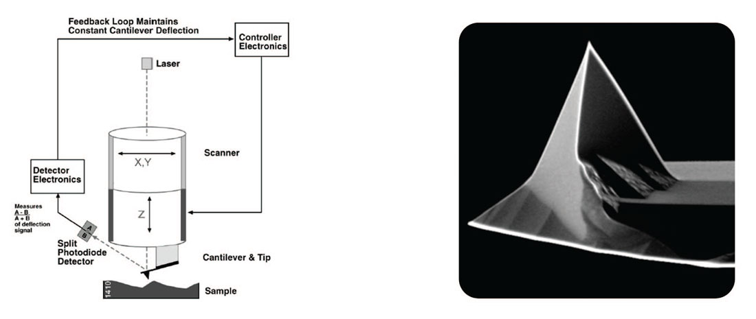 |
| Figure 2: AFM Schematic with feedback loop and typical cantilever geometry. (click image to enlarge) |
| The ease of implementation of the NanoLens provides a powerful compliment to Bruker’s 3D optical microscope capabilities. The NanoLens AFM can be easily co-aligned to the other objectives on the microscope system for fastest high-resolution inspection of an area of interest. |
| No special sample preparation is needed to measure a wide range of surface topography and properties. Additionally, there is a built-in 8x objective lens (up to16x when viewed through Bruker 3D optical microscope zoom optics) that allows the user to view the sample-cantilever interaction via the 3D microscope camera to easily identify the measurement region. The NanoLens AFM provides an automated approach over a 5mm range, with a maximum scan range on samples of up to 22?m with angstrom resolution. The maximum X/Y scan range is 70µm, though this can be zoomed to a much higher resolution inspection to highlight much smaller regions of interest as well. |
| A precision, quick-release adapter for turret mounting allows for fastest cantilever exchange with micron-level position reproducibility. This reproducibility is facilitated by a cantilever groove design (shown in Figure 3) that provides a kinematic mounting interface, eliminating the need for laser alignment. |
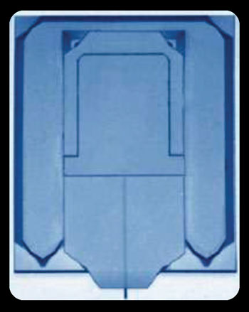 |
| Figure 3: Top view of cantilever chip seated in kinematic mounting interface. |
| Continue to next page (2 of 2) |
|
|

Become a Spotlight guest author! Join our large and growing group of guest contributors. Have you just published a scientific paper or have other exciting developments to share with the nanotechnology community? Here is how to publish on nanowerk.com. |
