| Posted: Feb 06, 2014 |
Integrated optical and AFM metrology (page 2 of 2) |
| Applications Example: Defect Inspection |
| The NanoLens AFM provides excellent surface information with sub-nanometer height resolution and typically less than 10nm lateral resolution. These capabilities provide a significant extension of the reach of 3D optical microscopes to “1000x” capability and beyond. |
| The following example shows how this powerful combination of 3D optical microscope speed and the flexibility of the co-aligned NanoLens AFM can be used for both identification and high-resolution detailed inspection. Figure 4 shows images of a surface area on a CD ROM disk, with a small black square indicating a candidate area for high-resolution NanoLens AFM inspection. |
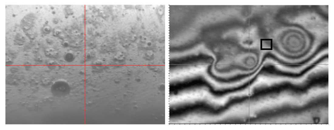 |
| Figure 4: Intensity image of CD ROM surface with contaminants shown at 16X magnification through integrated 8X optics and 2X FOV modifier lens (top). 50X interferometric objective intensity image near same site (bottom). Note hint of surface pits. (click image to enlarge) |
| Upon identification of such a region of interest, 3D surface measurements at that location are straightforward with the combination Bruker 3D microscope and NanoLens AFM toolset. For example, optical inspection at 50x magnification may be of interest for such an area. An example 3D microscope image of the area on the CD ROM surface pictured in Figure 4 is shown in Figure 5. |
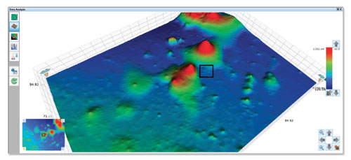 |
| Figure 5: 3D representation from 50x objective inspection on CD ROM surface. The black square represents area of interest for extended NanoLens AFM inspection. |
| 3D Microscope and AFM Combined System Advantage Once optical measurement is made at a particular area of interest, the full benefit of the NanoLens AFM can be realized. The turret-mounted NanoLens can be moved into position (it is co-aligned with the other objectives available on the 3D optical microscope head) and a direct measurement can be made on the region of interest, without moving the sample. |
| Figure 6 details the NanoLens AFM in the process of image acquisition. The scanning of the cantilever can be observed while the image is produced for the square area depicted previously. A progress bar is shown directly in Vision64™ software to let the user know what portion of the measurement is complete. |
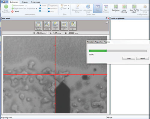 |
| Figure 6: NanoLens AFM inspection of area of interest in progress. |
| The image in Figure 7 was produced via dynamic force measurement with the NanoLens AFM. The data bits in the CD surface are shown clearly, as well as some nonuniformity on the surface at small scales (in this case on the order of 10µm square area of interest). These small scale variations in topography are less than 500nm wide, even 100nm in some cases. These features are easily imaged using the NanoLens AFM. |
| An additional NanoLens advantage when measuring samples for inspection applications is the ability of phase imaging to differentiate between contamination and surface defects. Where organics or polymers are present on the surface, variations in material that are nearly invisible in the topography scan, show up with high contrast in the phase images. |
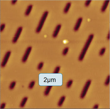 |
| Figure 7: High-resolution NanoLens AFM image of CD surface, including data bits. |
| Additionally, steep surface topography with small absolute height levels is resolved quickly and easily. The NanoLens AFM can also be applied to resolve inaccuracies in optical system measurements that may occur due to narrow line width spacing, dissimilar materials, or the presence of thin films on the sample. Reverting to optical system functionality is easily accomplished via a turret move, and a correlation function can easily be applied directly in Vision64 software based on the NanoLens AFM data. |
| Conclusion |
| The NanoLens AFM integrated with Bruker 3D optical microscopes provides a significant extension of metrology capabilities. The addition of this “1000x” lens extends lateral resolution, eliminates dissimilar material and thin film issues, and provides immediate capability for co-aligned (parcentric) operation of optical and AFM technologies. |
| This co-location of complementary technologies provides efficiency and direct impact on time to data and a data benefit for critical inspection applications in a range of industries. Combining the two systems not only increases and enhances metrology capabilities, but also drastically improves the overall efficiency of the measurements. |
| The end result is a single, simple-to-use system providing superior accuracy and resolution for today’s research and manufacturing environments. |
| Download this Application Note as PDF |
| Authors: Roger Posusta, Senior Marketing Application Engineer, Bruker Nano Surfaces Division,[email protected]. Drew Griffin, Sales Application Scientist, Bruker Nano Surfaces Division, [email protected]. Matt Novak, Ph.D., Marketing Application Manager, Bruker Nano Surfaces Division, [email protected]. |
|
|

Become a Spotlight guest author! Join our large and growing group of guest contributors. Have you just published a scientific paper or have other exciting developments to share with the nanotechnology community? Here is how to publish on nanowerk.com. |
