| Jun 14, 2026 |
Engineered crystal pathways turn light pulses into synaptic memoryEngineered grain boundaries guide sulfur ions through a layered crystal, letting light create lasting synapse-like memory in an artificial device. |
| (Nanowerk Spotlight) A memory device can hold information in several physical ways. Some store electrical charge. Others rely on magnetism, atomic rearrangement, or ion motion. For artificial synapses, ion motion is especially useful because it can make a device change gradually rather than simply flip between on and off. |
| A synapse changes with use. A strong signal can leave a larger effect than a weak one, and repeated signals can build into a longer-lasting response. Ions can support that kind of behavior because they move slowly enough to leave a physical trace after the original stimulus has passed. |
| But ions need routes through a material. If those routes are scattered and irregular, the memory effect becomes hard to repeat. If there are no routes at all, the ions barely move. A better approach is to make the routes part of the crystal itself. |
| In Advanced Materials ("Designable van der Waals Crystal for Artificial Neuronal Cell Mimicking"), researchers report that approach in rhenium diselenide, or ReSe₂, a van der Waals crystal, meaning a material made from stacked atomic layers held together by weak interlayer forces. They treat its surface with argon and hydrogen sulfide plasma. The treatment reshapes the upper layers into many tiny crystalline grains, adds sulfur, and leaves the deeper crystal more intact. |
| That hybrid structure gives the device its working architecture. The modified top region supplies dense grain boundaries, while the underlying layered crystal preserves an ordered base. The boundaries between the new grains act as pathways for sulfur ions. Instead of treating those internal borders as unwanted flaws, the device uses them to control where ions can move. |
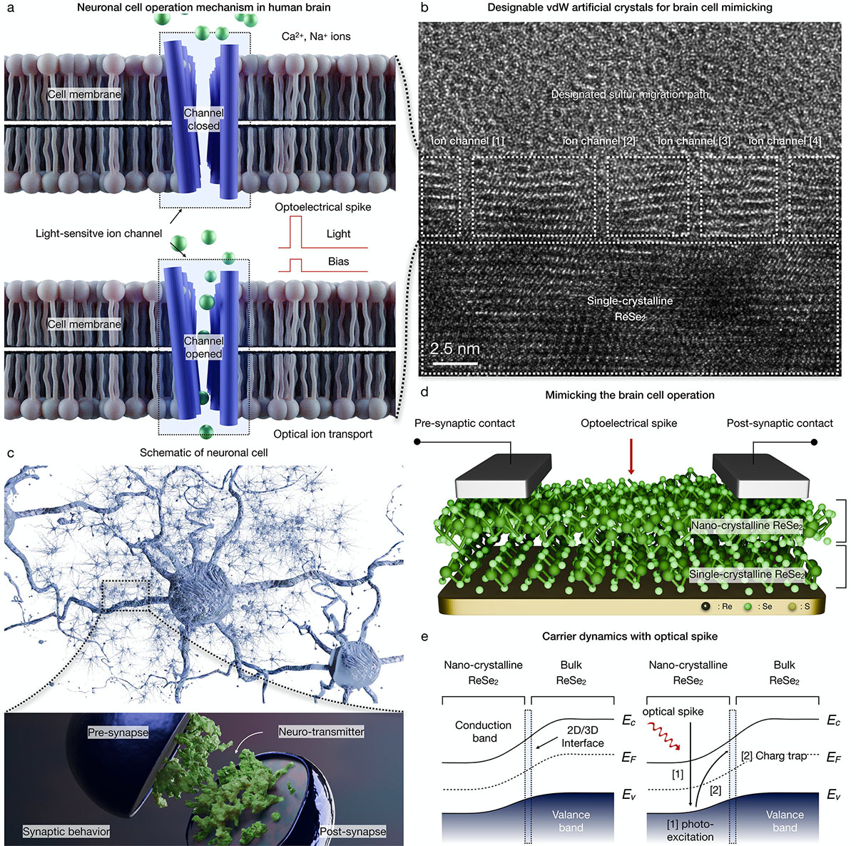 |
| Designable van der Waals (vdW) crystal for mimicking the neuronal light-sensitive ion channel. (a) Schematic illustration of the neuronal cell operation mechanism, migrating the Ca2+ and Na+ ion through light-sensitive ion channel. (b) Cross-sectional TEM image of nano-crystallized ReSe₂ crystal, mimicking the cross-sectional configuration of light-sensitive ion channel in neuronal cell membrane. (c) Schematic of a neuron and synapse, operating with transmission of the action potential. After initiation of the external stimulation, neurons transmit signal further to other neurons. (d) Structural configuration of vdW optoelectronic synaptic device for mimicking the brain cell operation, consisting of pre-synaptic contact, post-synaptic contact, and optoelectrical spike in nano-crystallized ReSe₂. (e) Sequential carrier dynamics of the photo-excitation process and the charge-trap mechanism in nano-crystallized ReSe₂. (click on image to enlarge) |
| When light hits the treated ReSe₂, electrons and holes appear first. These fast-moving carriers change how easily current flows. Sulfur ions then move more slowly along the grain-boundary pathways. Their motion helps preserve part of the light response as a longer-lived change in conductance, which is the ease with which current passes through the device. |
| A simple photodetector mainly reports that light is present. The nanocrystalline ReSe₂ device also records something about recent stimulation. Its conductance depends not only on the current light pulse, but also on the charge trapping and ion movement left behind by earlier pulses. |
| After treatment, the upper region contains sulfur, breaks into nanocrystalline grains, and carries current mainly through the grain-boundary network. The material therefore gains the kind of internal pathways needed for guided ion motion, rather than becoming a uniformly damaged crystal. |
| The sulfur-rich grain boundaries also change the transport mechanism. As the sulfurization conditions become stronger, the device shifts from one governed mainly by electronic carriers to one governed mainly by ion motion. Under the strongest reported condition, ion transport accounts for 95.61% of the combined carrier and ion contribution. |
| Repeated light pulses turn that two-speed response into gradual conductance updates. The device produces multiple intermediate states rather than a single on or off output. It shows long-term potentiation and long-term depression, which correspond to strengthening and weakening of a synaptic weight. It also shows paired-pulse facilitation, where closely spaced pulses produce a stronger response than isolated ones. |
| Changing the optical stimulation shifts the device response from short-term to long-term memory behavior. Weak or brief stimulation raises conductance only temporarily. Stronger or repeated stimulation produces a more persistent state. In the mechanism proposed by the researchers, light-generated carriers create the immediate change, while trapped charges and sulfur ion motion help stabilize the longer-lasting state. |
| Comparisons with other treated forms of ReSe₂ sharpen the role of the grain-boundary network. Material that is only destabilized, or material that contains sulfur without the same nanocrystalline channel structure, produces weaker and less balanced synaptic responses. The strongest behavior appears when the crystal contains both sulfur and dense grain boundaries. That points to designed internal routes, not general damage, as the source of the memory effect. |
| The same structure also affects relearning after partial forgetting. After an initial stimulation period, the current partly fades. When the researchers stimulate the device again, nanocrystalline ReSe₂ recovers a prior conductance level with fewer pulses than bulk ReSe₂. The paper reports a 34.7% improvement in retention efficiency, consistent with a partial physical record left by trapped charges and sulfur-ion arrangements. |
| That residual memory matters because artificial synapses need more than stable on and off states. They need intermediate weights that can strengthen, weaken, fade, and recover in response to recent inputs. In this device, the memory state comes from a coupled electronic and ionic process. Fast carriers provide sensitivity to light, while slower sulfur ion motion gives the material a more durable history. |
| Those gradual conductance updates also need to matter beyond a single device curve. In neuromorphic computing, conductance states can represent adjustable weights that filter and classify signals. The researchers therefore move from device measurements to vision-related demonstrations, where useful computation depends on changing how image information passes through a network. |
| Using the measured synaptic response, they first demonstrate edge detection, a basic visual-processing operation that highlights boundaries in an image. They then use the experimentally measured conductance states in a CIFAR-10 image-recognition demonstration and report 96.24% accuracy. That result does not amount to a finished artificial-vision chip. It shows that the device’s conductance updates can serve as useful weights in a vision model. |
| The broader lesson is that internal boundaries in a crystal can become functional parts of a device when their role is defined by the material design. In this case, grain boundaries guide sulfur ions through a layered crystal, while light-generated charges provide the faster response. The synaptic behavior comes from the combination of those two processes, not from either one alone. |
| A practical neuromorphic vision system would still need large arrays of consistent devices, integration with conventional electronics, and stable operation over extended use. The paper does not resolve those engineering challenges. Its contribution is to show that artificial synaptic behavior can be built into a crystal by designing where ions move. |
 By
Michael
Berger
– Michael is author of four books by the Royal Society of Chemistry:
Nano-Society: Pushing the Boundaries of Technology (2009),
Nanotechnology: The Future is Tiny (2016),
Nanoengineering: The Skills and Tools Making Technology Invisible (2019), and
Waste not! How Nanotechnologies Can Increase Efficiencies Throughout Society (2025)
Copyright ©
Nanowerk LLC
By
Michael
Berger
– Michael is author of four books by the Royal Society of Chemistry:
Nano-Society: Pushing the Boundaries of Technology (2009),
Nanotechnology: The Future is Tiny (2016),
Nanoengineering: The Skills and Tools Making Technology Invisible (2019), and
Waste not! How Nanotechnologies Can Increase Efficiencies Throughout Society (2025)
Copyright ©
Nanowerk LLC
|
|
ORCID information
|

Become a Spotlight guest author! Join our large and growing group of guest contributors. Have you just published a scientific paper or have other exciting developments to share with the nanotechnology community? Here is how to publish on nanowerk.com. |
