| Jun 30, 2026 |
Microwells make nano-LED assembly precise enough for AR and VR displaysTiny wells guide nano-LEDs into place, helping turn millions of small light sources into sharper headset display pixels. |
| (Nanowerk Spotlight) In a headset display, each pixel, the smallest controllable unit of an image, has to disappear into the scene. When it is too large, it does not just lower resolution. It turns the image into a visible grid of light sources rather than a continuous view. Near-eye optics make that grid hard to hide because they place the display close to the viewer and magnify its pixel structure. |
| Eliminating that visible grid pushes AR and VR displays toward pixel densities on the order of 2000 pixels per inch, several times the linear density of many high-end smartphone displays. Apple, for example, lists the iPhone 16 Pro at 460 pixels per inch. At headset-display densities, smaller light sources are necessary but not sufficient. The space available for each emitter shrinks, and so does the tolerance for placing it. |
| Inorganic LEDs fit the optical demands of near-eye displays because they can produce high brightness, respond quickly, and operate longer than organic emitters under demanding current conditions. Prior work on nanoscale LEDs for AR and VR light engines shows why shrinking LED geometry remains attractive for compact displays. The limiting issue is not the light they produce. It is the difficulty of turning millions of separate emitters into a dense, addressable array after they leave the wafer where they were grown. |
| The slow route is to pick up the LEDs and place them one by one. That can provide accuracy, but it becomes hard to scale when a display needs millions of emitters. The faster route is to move many devices at once through a liquid. That parallelism is attractive, but it gives up some direct mechanical control at the exact moment when each landing position matters most. |
| At nano-LED dimensions, the liquid becomes part of the manufacturing problem. Rod-shaped emitters can drift, rotate, stick to surfaces, or interact with neighboring rods before they settle. A weak force leaves sites empty. A stronger force can pull more than one emitter into the same location. A rod that stops a fraction of a micrometer away from its intended position can later sit outside the contact window that should turn it on. |
| A study in Advanced Functional Materials ("High‐Accuracy and Ultrahigh‐Density Electrofluidic Integration of Miniaturized LEDs for AR/VR Displays") approaches the task as a sorting problem. The researchers used blue indium gallium nitride and gallium nitride nano-LEDs shaped as short rods. Once released from a 4-inch sapphire wafer into acetone, the emitters became movable particles in a liquid stream. The substrate then had to direct those particles into predefined pixel sites instead of letting them collect wherever the flow and electric field carried them. |
| Alternating electric fields supplied the first part of that control. The field polarized the rods and pulled them toward places where the field changed most sharply. This motion, known as dielectrophoresis, also helped rotate the rods so their long axes followed the field direction. But attraction alone still left too many possible final positions. A display pixel needs a destination, not just a force drawing material toward it. |
| The recessed microwell provided that destination. Each well reshaped the local electric field and gave the incoming rod a confined place to settle. In a wider opening, a rod could shift, tilt, or leave room for another emitter. In the tighter geometry, the first rod occupied most of the useful space. The same site then became less favorable for additional capture, which helped turn a many-particle flow into one-emitter placement. |
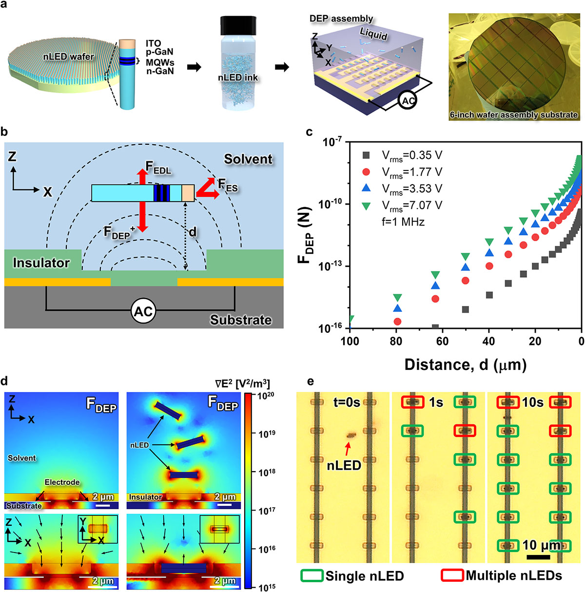 |
| Dielectrophoretic force-based assembly of nLEDs. (a) Schematic illustration of the DEP assembly process. (b) Dielectrophoretic and electrostatic forces acting on nLED during assembly. (c) The DEP force rapidly captures an nLED within seconds at designated positions. (d) The introduction of a recessed microwell generates a spatially resolved electric field gradient, enhancing the assembly performance. (e) DEP force calculated at different z-axis positions of an nLED under various applied voltages. (Image: Reproduced with permission from Wiley-VCH Verlag) (click on image to enlarge) |
| The same field that filled a well could also overfill it. Increasing the electric field improved capture only until the attractive region spread too far. Increasing the particle concentration improved supply only until rods began forming chains or crowding into occupied sites. The best performance came from matching field strength, particle supply, and well dimensions so that empty wells attracted rods while filled wells resisted them. |
| Under those conditions, the process reached an average assembly yield of 99.74% on substrates exceeding 5000 pixels per inch. Automatic optical inspection evaluated 8 813 981 assembly sites across a centimeter-scale substrate at 5225 pixels per inch, rather than relying on selected microscope views. The reported yield therefore reflects both local assembly behavior and large-area uniformity. |
| Precision carried the other half of the claim. In the optimized wells, the average placement offset reached about 0.06 µm, and nearly all successfully occupied wells kept their emitters within 0.5 µm of the intended position. Those offsets are small enough to matter for fabrication, because the assembled rods still had to survive contact formation rather than remain a static array for imaging. |
| The researchers added transparent indium tin oxide contacts after assembly so current could reach the ends of the rods. A misplaced nano-LED could cause that contact to miss the intended end region or reach into the active light-emitting layers. The tight alignment avoided that failure closely enough to produce working devices. |
| The finished blue panel contained 959 520 nano-LEDs across a 14 × 15 mm² area at 2936 pixels per inch. The devices showed low leakage current and stable blue electroluminescence over the tested current range, linking liquid assembly to electrical operation. The demonstration remains limited to blue emission, so full-color systems will still need red and green emitters or reliable micro-LED color-conversion pixels. |
| It also stops short of a fully integrated silicon backplane system, but it proves the step that had to come first: nano-LEDs can be assembled densely enough, accurately enough, and uniformly enough to remain useful after wiring. For AR and VR displays, that is the difference between making smaller emitters and making smaller working pixels. |
 By
Michael
Berger
– Michael is author of four books by the Royal Society of Chemistry:
Nano-Society: Pushing the Boundaries of Technology (2009),
Nanotechnology: The Future is Tiny (2016),
Nanoengineering: The Skills and Tools Making Technology Invisible (2019), and
Waste not! How Nanotechnologies Can Increase Efficiencies Throughout Society (2025)
Copyright ©
Nanowerk LLC
By
Michael
Berger
– Michael is author of four books by the Royal Society of Chemistry:
Nano-Society: Pushing the Boundaries of Technology (2009),
Nanotechnology: The Future is Tiny (2016),
Nanoengineering: The Skills and Tools Making Technology Invisible (2019), and
Waste not! How Nanotechnologies Can Increase Efficiencies Throughout Society (2025)
Copyright ©
Nanowerk LLC
|
|
|

Become a Spotlight guest author! Join our large and growing group of guest contributors. Have you just published a scientific paper or have other exciting developments to share with the nanotechnology community? Here is how to publish on nanowerk.com. |
