| Jun 20, 2026 |
Carbon nanotube transistors turn invisible infrared light into memoryA carbon nanotube transistor turns invisible 940 nm light into both a signal and memory, advancing low-power neuromorphic vision hardware. |
| (Nanowerk Spotlight) When a scene is too dark for a conventional camera, the usual fix is to add illumination. That can solve the imaging problem while creating a new one: the light itself may alert people, disturb animals, interfere with instruments, or change the conditions a monitoring system is trying to observe. |
| Near-infrared light can brighten a scene for a sensor while remaining invisible to human eyes. That makes it useful in night-vision systems, security cameras, depth sensing, and some biomedical imaging, including broader work on neuromorphic night vision. The sensor still has to respond strongly to that invisible light, and many light-sensitive devices lose performance where that invisibility becomes most useful. |
| Some image sensors are being designed to do more than record light. The goal, also explored in work on optoelectronic transistors for artificial vision, is to let the sensing material begin processing visual information where light first arrives, so less raw data has to move to a separate processor. That requires a controllable electrical memory: each pulse of light should leave a trace, and repeated pulses should strengthen or weaken it. |
| Devices with this behavior are called optoelectronic synaptic devices. They combine light sensing with synapse-like changes in electrical conductance, but many respond more strongly to ultraviolet or visible light than to the deeper near-infrared wavelengths used for unobtrusive illumination. |
| A paper in Advanced Functional Materials ("Carbon Nanotube‐Based Optoelectronic Synaptic Thin‐Film Transistors at 940 Nm for Covert Neuromorphic Visual Surveillance and Image Recognition") targets that mismatch at 940 nm, a wavelength outside human vision. |
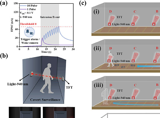 |
| Intrusion detection and event mapping using IEICO-4F/SWCNT photosynaptic TFTs. (a) EPSC-based intrusion event identification and alarm triggering. (b) 940 nm NIR intrusion monitoring in nighttime covert spaces: invisible to the human eye but perceptible to TFTs. (c) Intrusion event detection using a IEICO-4F/SWCNT TFT array under 940-nm illumination. (Image: Reproduced with permission from Wiley-VCH Verlag) |
| The device combines semiconducting single-walled carbon nanotubes with IEICO-4F, an organic molecule that absorbs near-infrared light. The nanotubes form the transistor channel, the path that carries current. They offer strong electrical properties and fit thin-film electronics, but a sparse nanotube network absorbs little light on its own. It needs a partner that can convert the target wavelength into electrical change. |
| IEICO-4F provides that conversion. In a solid film, its molecules pack in a way that shifts strong absorption toward the near-infrared region, close to 940 nm. Light at that wavelength creates mobile charges in the molecular layer. Some of those charges enter or influence the nanotube channel, changing the current that flows through the transistor. |
| Among the tested wavelengths, 940 nm pulses produced the strongest synaptic current response. Repeated pulses made the current change larger and more persistent, so recent optical history became encoded as conductance rather than lost after each exposure. The device could therefore register invisible illumination while also retaining information about how often and how strongly that illumination arrived. |
| The retained signal comes from charges that remain after the light switches off. Illumination creates mobile electrical charges in the IEICO-4F layer. Some contribute to current in the nanotube channel, while others become stuck in defect states in the aluminum oxide dielectric or near the channel interface. Those trapped charges keep influencing the channel and preserve a temporary electrical trace of the light pulse. |
| A gate voltage can release trapped charge and return the device toward its original state. Light writes the state, current reads it, and an electrical pulse resets it. That operating cycle gives the transistor local sensing and memory in the same structure, which is the function needed for a neuromorphic visual front end. |
| The synaptic effects also capture timing. In paired-pulse facilitation, a second light pulse produces a stronger response than the first when it arrives soon enough. With more pulses, wider pulses, or more frequent pulses, the device shifts from short-lived changes toward longer-lasting plasticity. Timing and repetition become part of the electrical signal rather than details that disappear after detection. |
| Energy use requires careful interpretation. The study reports synaptic energy consumption as low as 54.8 aJ per event under very low bias, but that lowest value occurs at a wavelength with a weaker response. At 940 nm, where the device responds most strongly, the energy per pulse is higher. A stronger current response requires more carrier motion, and that costs energy. |
| The transistors retained their photosynaptic response after 30 days in ambient air without encapsulation, with only slight decay. That does not establish outdoor durability or long-term product reliability. It does show that the IEICO-4F coated nanotube channel can keep functioning after ordinary storage, and that the light-sensitive interface does not fail immediately outside freshly fabricated test conditions. |
| The clearest demonstration used 940 nm light as an invisible optical tripwire. Near-infrared pulses pushed the transistor current above a preset threshold when the beam reached the device. An object crossing the path blocked some pulses, keeping the current below the threshold. With multiple sensing points, the system inferred simple indoor movement from which invisible beams had been interrupted. |
| Measured conductance states from the transistors also served as weights in neural-network simulations. A spiking neural network reached 96.63% accuracy on handwritten digit recognition. A convolutional neural network reached 91.37% accuracy for aircraft recognition under 940 nm illumination. These results show that the device states can support computation, not that the researchers have built a complete neuromorphic camera. |
| The work does not yet deliver a large imaging array, real-time on-chip recognition, or a packaged monitoring system. Scaling the devices, integrating readout circuits, protecting the organic layer, and testing under complex lighting remain open engineering tasks. Its main contribution is a transistor channel that can convert 940 nm illumination into both a current signal and a temporary memory state. |
 By
Michael
Berger
– Michael is author of four books by the Royal Society of Chemistry:
Nano-Society: Pushing the Boundaries of Technology (2009),
Nanotechnology: The Future is Tiny (2016),
Nanoengineering: The Skills and Tools Making Technology Invisible (2019), and
Waste not! How Nanotechnologies Can Increase Efficiencies Throughout Society (2025)
Copyright ©
Nanowerk LLC
By
Michael
Berger
– Michael is author of four books by the Royal Society of Chemistry:
Nano-Society: Pushing the Boundaries of Technology (2009),
Nanotechnology: The Future is Tiny (2016),
Nanoengineering: The Skills and Tools Making Technology Invisible (2019), and
Waste not! How Nanotechnologies Can Increase Efficiencies Throughout Society (2025)
Copyright ©
Nanowerk LLC
|
|
ORCID information
|

Become a Spotlight guest author! Join our large and growing group of guest contributors. Have you just published a scientific paper or have other exciting developments to share with the nanotechnology community? Here is how to publish on nanowerk.com. |
