| Jul 06, 2026 |
Ion-beam origami unlocks wafer-scale 3D photonic systemsBroad-beam ion etching folds flat nanostructures into 3D photonic devices across a 4-inch wafer while preserving speed, uniformity, and optical function. |
| (Nanowerk Spotlight) 3D photonic devices face a manufacturing trade-off that has been difficult to escape. Methods that shape nanostructures with high precision usually work too slowly and locally for wafer-scale production. Wafer-scale processes, in turn, usually lack the control needed to build precise out-of-plane geometry. |
| Planar nanofabrication handles one side of the problem well, patterning dense optical structures across large substrates with nanometer-scale accuracy. But many optical functions depend on height, curvature, and handedness, not only on features drawn in a plane. |
| That extra dimension changes what a device can do. A lifted segment can make a structure respond differently to left-handed and right-handed circularly polarized light. A curved grating can shift a visible resonance. These effects matter for chiral sensing, tunable filters, and compact optical components, but only if thousands or millions of repeated structures bend in the same way. Small deviations in angle or curvature can turn a designed optical response into a patchwork of mismatched ones. |
| Existing folding methods have solved only parts of the problem. Capillary forces, residual stress, compression buckling, and related approaches such as kirigami-style nanostructure fabrication can reshape patterned films, but these routes often depend on material-specific mechanics or external actuation. |
| Focused ion beams can bend nanoscale structures with high precision, but they write serially. As the beam scans across a device, earlier regions deform before later regions receive the same exposure, making large-area uniformity harder to preserve. |
| A paper in Advanced Materials ("Unlocking Wafer‐Scale 3D Photonic Systems With Ion‐Beam‐Induced Origami") reports a broad-beam ion beam etching approach that addresses this trade-off. Instead of writing one feature at a time, the method exposes a patterned 4-inch wafer to a uniform argon ion beam, folding flat nanostructures into stable 3D photonic architectures in a parallel step. |
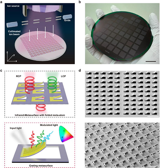 |
| Principle and parallel fabrication characteristics of broad-beam ion-beam etching (IBE). (a) Schematic illustration of the wafer-scale 3D origami fabrication process via broad-beam IBE. (b) Photograph of a fully processed 4-inch wafer, demonstrating uniform 3D transformation across the entire substrate. (c) Conceptual illustrations of the two distinct functional photonic devices fabricated in this work: a chiral 3D bending metasurface for mid-infrared circular dichroism (top) and a tunable collectively-buckled plasmonic grating supporting bound states in the continuum (BICs) for the visible spectrum (bottom). The symbols in the phase diagram mark the locations of the modulated light. (d) SEM images of other 3D fabricated structures on the wafer, with the bottom image showing the bending configuration of an η-shaped structure. Scale bars are 0.5 inch for optical images in (b), 30 µm for the top and 200 µm for the bottom image in (d), respectively. (Image: Reproduced with permission from Wiley-VCH Verlag) |
| The method works by turning ion damage into a controlled mechanical force. The starting structures sit on suspended silicon nitride membranes carrying thin gold patterns. When argon ions strike the surface, most of the defects form near the top of the film. That damaged surface layer wants to expand more than the material beneath it. Because the structure is suspended, the mismatch bends the film instead of remaining locked inside a flat sheet. |
| For photonics, bending must behave like a design parameter, not an isolated mechanical effect. In cantilever arrays, the bending angle followed the length of the gold and silicon nitride structures under fixed irradiation conditions. Width had much less influence for structures of the same length. That relationship gives designers a practical handle: change the planar geometry, and the final 3D angle changes in a predictable way. |
| The difference between serial and parallel folding becomes clearer as the patterned area grows. Focused ion beam processing can produce precise 3D structures in small regions, but larger patterns accumulate drift, stage errors, dose variation, and exposure-history effects. Broad-beam ion etching removes the writing sequence from the problem. Equivalent structures receive the same dose at the same time, and the reported angular uniformity remains above 97%. |
| The time scale matters for the same reason. The ion step reshaped patterned structures in 10 to 20 seconds, while focused ion beam processing takes minutes for much smaller regions and slows further as the area grows. Faster fabrication is only part of the gain. The larger point is that parallel exposure preserves geometric consistency while moving from isolated structures toward wafer-scale optical systems. |
| Uniform folding would mean little if it only produced neat mechanical shapes. The folded structures also have to change light in ways that flat versions cannot. Handedness gives one of the clearest tests. A flat metal pattern can concentrate optical fields, but lifting part of the structure out of the plane creates a 3D asymmetry that can separate left-handed and right-handed circular polarization. |
| The device sits within broader advances in chiral nanophotonics, where engineered metasurfaces strengthen interactions with circularly polarized light. Here, the key distinction is that the handed response comes from a 3D geometry created across a wafer by a parallel ion process. |
| The handed response comes from split-ring resonators, metal patterns that interact strongly with infrared light. In the planar state, the rings provide the needed subwavelength layout but not the full 3D geometry. Ion exposure lifts one segment of each resonator upward. That vertical displacement links the electric and magnetic responses inside each unit, giving the array a handed optical response rather than only a patterned surface. |
| The folded metasurface reaches a circular dichroism value of 0.8 at 3.41 µm. Circular dichroism measures how differently a structure transmits left-handed and right-handed circularly polarized light. A value at this level indicates strong polarization selectivity, and the close match with simulation links that response to the programmed out-of-plane shape. |
| The same ion exposure can also bend an entire optical surface. In a suspended gold grating on silicon nitride, irradiation curves the grating and changes how its periodic metal lines meet incoming visible light. As curvature increases, the reflected color shifts toward blue under white-light illumination. The visible color shift matches a measurable movement in the grating’s optical resonance. |
| Across the curved grating, the resonance moves from about 650 nm to 500 nm. Under a controlled comparison, the resonance dip shows a 100 nm blue shift. The broader range reflects position-dependent curvature across the device, while the controlled shift isolates the change under comparable measurement conditions. The result extends the process beyond static 3D shaping into visible optical tuning. |
| The two devices make the same point at different scales. One uses local deformation of repeated meta-atoms to generate chirality in the mid-infrared. The other uses global curvature of a grating to tune a visible resonance. Both start from accurate planar patterns and gain optical function after broad-beam ion exposure moves those patterns into the third dimension. |
| That makes the approach complementary to existing nanophotonic manufacturing rather than a replacement for it. Planar lithography still creates the starting patterns. Broad-beam ion etching adds a post-patterning transformation that changes their vertical form. Many metasurfaces and integrated optical components already depend on mature flat processing, so a practical 3D route becomes more valuable when it preserves that foundation. |
| The method’s main limitation follows directly from its strength. Uniform exposure produces fast and consistent wafer-scale bending, but future devices may need neighboring regions to fold by different amounts or stay flat. The paper identifies limited programmability, limited spatial selectivity, and the lack of direct site-specific dose control as open problems. A process that succeeds by treating the wafer evenly must still learn to create controlled local differences. |
| Masking offers one route around that constraint. Physical stencil masks could shield selected areas while exposing others. Masks made by focused ion beam, electron beam lithography, or ultraviolet lithography could define smaller regions and more complex exposure patterns. Stacked masks could let different parts of a wafer receive different doses while keeping the high-throughput character of broad-beam processing. |
| The result does not make every 3D photonic design manufacturable. But it does show that out-of-plane reshaping can fit the scale logic of chip fabrication. Focused ion beams established that ions can bend nanostructures with precision. Broad-beam ion etching shows that bending can become parallel, uniform, and fast. The next barrier is local programming that does not sacrifice the parallel exposure that makes the approach useful at wafer scale. |
 By
Michael
Berger
– Michael is author of four books by the Royal Society of Chemistry:
Nano-Society: Pushing the Boundaries of Technology (2009),
Nanotechnology: The Future is Tiny (2016),
Nanoengineering: The Skills and Tools Making Technology Invisible (2019), and
Waste not! How Nanotechnologies Can Increase Efficiencies Throughout Society (2025)
Copyright ©
Nanowerk LLC
By
Michael
Berger
– Michael is author of four books by the Royal Society of Chemistry:
Nano-Society: Pushing the Boundaries of Technology (2009),
Nanotechnology: The Future is Tiny (2016),
Nanoengineering: The Skills and Tools Making Technology Invisible (2019), and
Waste not! How Nanotechnologies Can Increase Efficiencies Throughout Society (2025)
Copyright ©
Nanowerk LLC
|

ORCID information
|

Become a Spotlight guest author! Join our large and growing group of guest contributors. Have you just published a scientific paper or have other exciting developments to share with the nanotechnology community? Here is how to publish on nanowerk.com. |