| Jun 25, 2026 |
New printing method sharpens quantum dot display pixelsA controlled printing instability creates sharper quantum dot patterns and helps prevent charge leakage in high-resolution QLED displays. |
| (Nanowerk Spotlight) Augmented-reality glasses and near-eye microdisplays need tightly packed light-emitting pixels. At that scale, a pattern can fail even when it looks correctly drawn. A narrow quantum dot line is not enough if its thickness varies, its edge leaks current, or fabrication residues reduce light output. |
| Quantum dot light-emitting diodes, or QLEDs, sharpen that manufacturing problem. Quantum dots emit narrow, tunable colors under electrical drive, which makes them useful for compact displays with high color purity. Recent progress in flexible quantum dot displays shows why these materials appeal to compact and mechanically adaptable formats, but their colors only remain separate if each emitting material sits in a cleanly bounded, electrically isolated region. |
| Patterning tools already exist, but each route gives up something essential. Simple, maskless printing protects the material and continues to improve, as recent work on inkjet-printed QLEDs shows, but it still struggles to draw uniform micrometer-scale features. Template-based methods can sharpen the geometry, but masks, wet processing, residues, and transfer steps can compromise the light-emitting layer. Electrohydrodynamic printing removes the template, yet shifts the difficulty to jet stability and throughput. |
| In Advanced Materials ("Direct Writing High‐Resolution Quantum Dot Micro‐Patterns: Toward High‐Performance Electroluminescence Behavior"), researchers report a template-free direct writing method that turns controlled liquid-film breakup into a way to pattern quantum dots. A conical fiber array guides a quantum dot solution across a heated substrate, forming micro-lines 2 µm wide over about 10 cm². The uneven thickness is not treated as a flaw. Paired with a complementary PMMA polymer layer, it helps steer charge into the emitting lines and suppress leakage between them. |
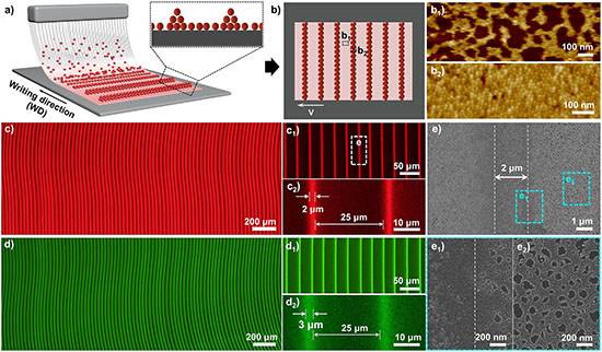 |
| Micro-patterning QDs by a template-free direct writing strategy. (a) Schematic cartoon of the CFA-guided direct writing process for fabricating micro-patterned QDs films on a properly heated substrate. (b) The cartoon of the as-prepared QDs micro-pattern, where QDs are tightly packed into ultrafine micro-lines array that are periodically parallel in one direction. The morphology of regions (b1) and (b2) was characterized by the atomic force microscope (AFM). (c, d) The fluorescence images of the as-prepared micro-patterned R- and G-QDs taken at different magnification, showing highly ordered micro-line array with a linewidth of 2 µm. The magnified pictures evidence their structure by a rather thin QDs layers in between of micro-lines (c1, c2, d1, and d2). (e) The scanning electron microscope (SEM) images of micro-patterned QD film at the micro-lines (e1) and the spacing (e2). (Image: Reproduced with permission from Wiley-VCH Verlag) |
| The method works because the researchers control a drying behavior that usually ruins coating quality. As solvent evaporates from a thin liquid film, particles tend to gather where liquid, solid, and air meet. That moving edge can leave ridges, gaps, or patchy deposits. Here, the process repeats with enough regularity to write ordered quantum dot lines instead of random drying marks. |
| The conical fiber array keeps the liquid supply steady while the heated substrate pulls solvent away near the moving front. Quantum dots concentrate at the contact line, and capillary flow draws more material into the same region. The contact line pins, builds a thicker deposit, breaks free, and moves forward. The next pinning event starts the same cycle again. |
| That rhythm only appears when several conditions match. Heating must be strong enough to drive patterned deposition, but not so strong that it scatters the material. The writing speed must give the contact line time to pin without letting the deposit overgrow. The solvent and quantum dot concentration also shape whether the pattern becomes continuous, broken, or irregular. |
| Under optimized conditions, the process produced a periodic thickness pattern over a large area. Red quantum dots formed lines about 2 µm wide, while green quantum dots formed lines about 3 µm wide. Between the lines, the film did not become empty. It retained a much thinner quantum dot layer, creating a repeating thick-and-thin structure across the written region. |
| That structure matters because a display pixel is an electrical device, not just a printed shape. The researchers coated the patterned quantum dot film with polymethyl methacrylate, or PMMA, an insulating polymer. PMMA followed the surface topography in the opposite pattern. It formed a thinner layer above the thicker quantum dot lines and a thicker layer above the thinner regions between them. |
| The resulting bilayer created alternating regions with different charge access. Electrons could enter the thick quantum dot lines more easily through thinner PMMA. Between those lines, thicker PMMA suppressed unwanted electron injection into the thin quantum dot layer. The geometry turned a printed thickness variation into a way to choose where charge enters and where light forms. |
| Devices without PMMA showed why this charge control was necessary. Under voltage, leakage currents damaged the patterned QLEDs after short operation. With an appropriate PMMA layer, the devices reduced leakage while keeping charge injection strong enough for bright emission. Excessive PMMA blocked carriers too strongly, while insufficient PMMA left the structure more vulnerable to leakage. |
| The best red QLED reached an external quantum efficiency of 21.4% with 2 µm-wide emitting lines and a luminance of 7.5 × 10⁴ cd m⁻². The device maintained narrow red emission under different viewing angles and operating voltages. The same patterning strategy also produced green, blue, and cyan devices, pointing to broader color compatibility rather than a single-material result. |
| Efficient pixels also need to release the light they generate. Some emission normally remains trapped inside layered devices. In this architecture, the quantum dot and PMMA regions bend light differently, and their alternating structure helped extract light from optical waveguide modes. The paper reports a 14.1% increase in optical pickup rate, adding an optical gain to the charge-routing effect. |
| The advance lies in connecting pattern formation to device physics. The thickness contrast left by controlled liquid-film breakup helps define where charge recombines, turning a drying effect into part of the electroluminescent architecture. Commercial use would still require progress in full-color registration, yield, and lifetime, but the principle is clear: micrometer-scale QLED patterning can use fluid motion as a design tool rather than treating it only as a defect. |
 By
Michael
Berger
– Michael is author of four books by the Royal Society of Chemistry:
Nano-Society: Pushing the Boundaries of Technology (2009),
Nanotechnology: The Future is Tiny (2016),
Nanoengineering: The Skills and Tools Making Technology Invisible (2019), and
Waste not! How Nanotechnologies Can Increase Efficiencies Throughout Society (2025)
Copyright ©
Nanowerk LLC
By
Michael
Berger
– Michael is author of four books by the Royal Society of Chemistry:
Nano-Society: Pushing the Boundaries of Technology (2009),
Nanotechnology: The Future is Tiny (2016),
Nanoengineering: The Skills and Tools Making Technology Invisible (2019), and
Waste not! How Nanotechnologies Can Increase Efficiencies Throughout Society (2025)
Copyright ©
Nanowerk LLC
|
|
ORCID information
|

Become a Spotlight guest author! Join our large and growing group of guest contributors. Have you just published a scientific paper or have other exciting developments to share with the nanotechnology community? Here is how to publish on nanowerk.com. |
