| Jun 18, 2026 |
Nano-kirigami creates programmable optical pixels from folding goldNano-kirigami turns patterned gold films into folding optical pixels, pointing toward dense programmable arrays. |
| (Nanowerk Spotlight) The shape of a surface controls how it handles light. A smooth mirror sends a beam back in one direction. Bend that mirror or roughen it, and the reflected light changes direction or spreads out. A surface can therefore control light without changing the light source. Change the surface, and the optical response changes with it. |
| That idea becomes more powerful when different parts of the same surface can take on different shapes. One region can stay flat and reflect light cleanly, while another can bend and scatter it. The surface no longer acts as one optical element. It becomes a patterned optical surface, able to form visible shapes, encode information, or redirect light in selected areas. |
| The challenge is scale. A large moving mirror or shutter can switch light, but it cannot produce a detailed optical pattern unless the surface is divided into many smaller controllable elements. Each element must still move enough to change the light visibly, while also leaving room for electrical control. Shrink the elements too far, and motion, contrast, and wiring begin to compete for the same space. |
| That trade-off is the problem behind programmable optical arrays. They need many closely spaced light-control elements, each switching reliably between optical states. Writing in Advanced Materials ("Programmable Optical Megapixel Nano‐Kirigami Matrix"), researchers report a programmable optical matrix built from nano-kirigami, a nanoscale version of cut-and-fold mechanics. Instead of using a rigid micromirror, each optical unit is a patterned gold film that folds under voltage and changes how it scatters light. |
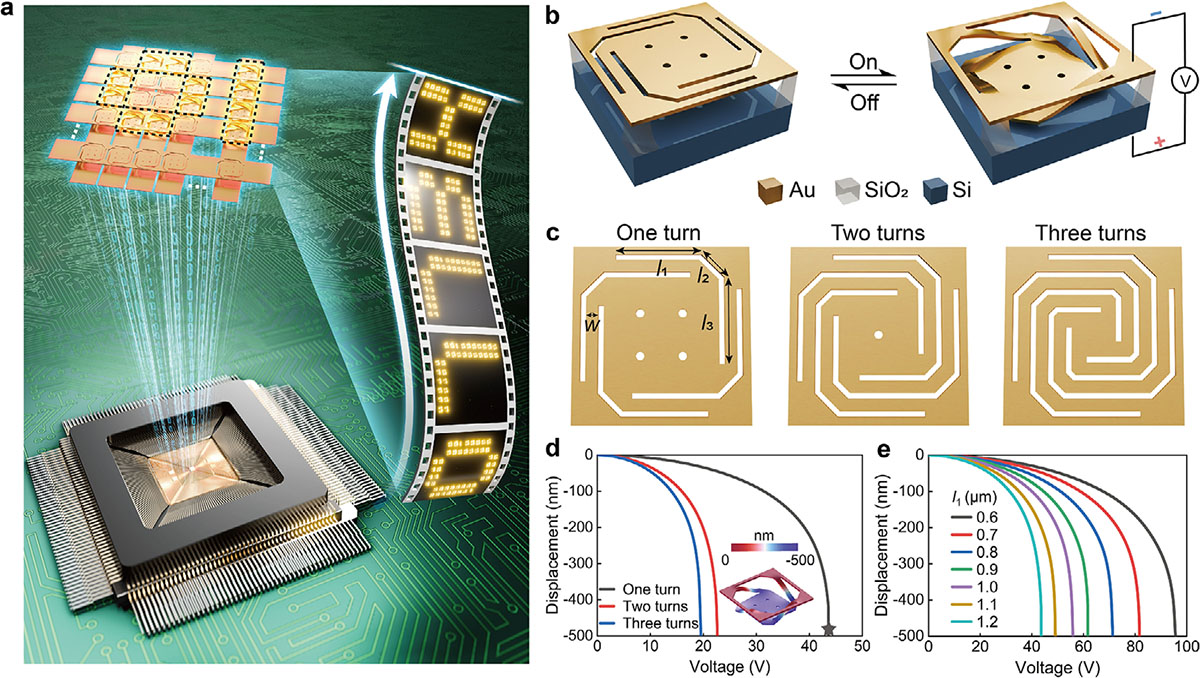 |
| Conceptual design of programmable optical nano-kirigami matrix with electromechanical deformations. (a) Schematic of the programmable optical nano-kirigami matrix for freely addressable information displays. (b) Schematic of a suspended turn-shaped nano-kirigami unit in flat state (voltage off) and deformation state (voltage on). The nano-kirigami unit consists of a central plate to induce an attractive electrostatic force and surrounded four arms to be deformed when the voltage is applied. (c) Top views of three turn-shaped nano-kirigami units with the designs of one turn, two turns, and three turns with different arm lengths, respectively, showing the shapes of high duty cycle. (d, e) Simulated deformation displacements of the electromechanically deformable turn-shaped units with different number of turns and varied arm lengths, respectively. (Image: Reproduced with permission from Wiley-VCH Verlag) (click on image to enlarge) |
| The basic unit starts as a suspended square of gold, cut so that a central plate connects to the surrounding film through slender arms. When voltage is applied between the gold and the silicon below it, electrostatic attraction pulls the plate downward. The arms bend with it. When the voltage is removed, their elasticity helps return the structure to its flatter starting state. |
| This motion gives the pixel a clear division of labor. The central plate supplies the area needed for a strong electrostatic pull and continues to reflect incoming light. The arms supply the motion, bending out of the original plane and scattering light more strongly after deformation. The optical signal changes because the structure physically reshapes the surface that the light encounters. |
| The researchers designed the main pixel as a turn-shaped pattern made from straight segments and sharp corners. Earlier kirigami-inspired nanoscale work had already shown how cut films could manipulate light at the nanoscale, but this study pushes the idea toward dense, electrically programmable optical arrays. The turn-shaped geometry fills more of the available pixel area than a smooth spiral cut, which matters because unused area contributes little to the optical switch. |
| A higher duty cycle gives each unit more working surface inside the same footprint. In a small optical array, that extra working area can separate a weak laboratory signal from a visible optical change. The experiments show how unforgiving this geometry can be. Two pixels made from the same material and driven at the same voltage behaved very differently because their arms had different lengths. |
| The shorter-arm version changed its reflection by only about 6% at 32 V. With longer arms, the modulation contrast rose above 60% across 400 to 1000 nm, including a substantial response in the visible range. More flexible structures moved more easily, but that did not automatically make them better display pixels. Adding turns to the arms lowered the voltage needed to pull the suspended gold downward. |
| It also made the visible-range response less stable. For the display experiments, the researchers used the one-turn design because it gave steadier optical contrast, even though it required stronger actuation. The first visual tests used that contrast difference to hide and reveal fixed patterns. High-contrast pixels traced the desired image, while low-contrast pixels filled the surrounding background. |
| With no voltage, the surface appeared blank because the two regions looked similar. When voltage was applied, the high-contrast regions scattered light differently and the hidden image emerged. Smiley faces, mazes, butterflies, and a rotating pinwheel appeared and disappeared this way. |
| Those demonstrations proved that folding gold structures could make switchable optical images, but the images were still built into the sample. A programmable display needs the ability to choose the pattern after fabrication. To reach that point, the researchers made a crossed-electrode matrix with 100 rows and 100 columns. A folding gold unit sat at each intersection, so selected voltages could address chosen points in the grid. |
| This matrix contained 10,000 individually addressable pixels. Its pitch was 4.8 µm, larger than the densest fixed-pattern arrays, but the added space allowed the row-and-column wiring needed for control. Under a dark-field microscope, selected pixels brightened while neighboring pixels remained dark. The same active area could show different letter patterns, with HELLO replaced by I LOVE through electrical programming rather than a change in the physical structure. |
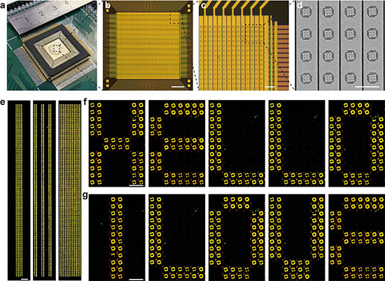 |
| Proof-of-concept demonstration of freely encoded information displays with 10,000 pixels. (a) Camera image of a fabricated structural array loaded on an electrical PCB. (b) Optical microscope image of fabricated nano-kirigami matrix with 10,000 pixels on the crossed electrodes of 100 rows and 100 columns. (c) Optical microscope image and (d) SEM image of a local region on the nano-kirigami matrix. (e) In-situ scattering optical images with programmed stripes under a dark-field microscope at v = 52 V (see details in Movie S5). (f, g) In-situ scattering images of the freely programmed characters “HELLO” and “I LOVE” displayed sequentially in the same area with a stroke width of two pixels under a dark-field microscope at v = 44 V (see details in Movie S6). All pixels consist of one-turn structures with l1 = 1.2 µm. Scale bars: (b) 100 µm; (d) 5 µm; (e) 20 µm; (c), (f-g) 10 µm. (Image: Reproduced with permission from Wiley-VCH Verlag) |
| The move from 10,000 addressable pixels to millions of optical units required a different architecture. The researchers fabricated a larger chip containing 3.87 million nano-kirigami units spaced at 2.5 µm. Instead of wiring each unit separately, they grouped the structures into 200 long stripe electrodes. Each stripe contained thousands of units that switched together. The result was a high-count optical matrix that could reconfigure information line by line, not pixel by pixel. |
| For this larger device, the researchers used a spiral nano-kirigami pattern rather than the turn-shaped design. The spiral geometry reduced the actuation voltage, allowing operation at 18 V in the reported optical tests. It also gave up some of the duty-cycle advantage that made the turn-shaped pixel optically stronger. The comparison reveals the central engineering compromise in the work: the design that scales most readily is not the one with the strongest individual-pixel performance. |
| Even with stripe-level control, the large matrix could transmit structured information. The researchers encoded words such as LIGHT and NATURE in Morse-code-like stripe patterns. They also used stripe sequences to represent notes from Twinkle, Twinkle, Little Star. These demonstrations do not amount to a full megapixel video display, but they do show that a dense field of folding optical units can be electrically reconfigured into readable information patterns. |
| The optical output was not confined to microscope images. In a simple projection setup, voltage-driven deformation scattered reflected light strongly enough to cast visible information onto a screen. Fixed turn-shaped arrays projected images such as a smiley face and butterfly, while the larger stripe-controlled matrix projected encoded text. That step matters because it moves the device from local reflectance measurements toward a practical optical function. |
| The 2.5 µm pitch gives the work its sharpest comparison with existing light-control hardware. The researchers compare it with state-of-the-art digital micromirror devices, which they list at a minimum pixel size of 5.4 µm. The comparison is useful but narrow. Digital micromirror devices are mature commercial systems with fast control electronics and established manufacturing. The nano-kirigami arrays show a smaller reported pitch, but not yet the same integrated performance. |
| The demonstrations stop short of a fully integrated display. The densest arrays show that nano-kirigami units can be packed below the pitch cited for state-of-the-art digital micromirror devices. The crossed-electrode matrix shows that selected units can be addressed individually. The megapixel device shows that millions of units can be fabricated and driven in groups. The missing step is a single architecture that combines those features without losing optical contrast or making the wiring impractical. |
 By
Michael
Berger
– Michael is author of four books by the Royal Society of Chemistry:
Nano-Society: Pushing the Boundaries of Technology (2009),
Nanotechnology: The Future is Tiny (2016),
Nanoengineering: The Skills and Tools Making Technology Invisible (2019), and
Waste not! How Nanotechnologies Can Increase Efficiencies Throughout Society (2025)
Copyright ©
Nanowerk LLC
By
Michael
Berger
– Michael is author of four books by the Royal Society of Chemistry:
Nano-Society: Pushing the Boundaries of Technology (2009),
Nanotechnology: The Future is Tiny (2016),
Nanoengineering: The Skills and Tools Making Technology Invisible (2019), and
Waste not! How Nanotechnologies Can Increase Efficiencies Throughout Society (2025)
Copyright ©
Nanowerk LLC
|
|
ORCID information
|

Become a Spotlight guest author! Join our large and growing group of guest contributors. Have you just published a scientific paper or have other exciting developments to share with the nanotechnology community? Here is how to publish on nanowerk.com. |
