| Posted: Mar 14, 2006 |
Large-scale fabrication of integrated nanoelectronic devices moves closer |
| (Nanowerk News) A new methodology for integrating nanowires with micropatterned substrates using directed assembly and nanoscale soldering was developed by researchers at Johns Hopkins University in Baltimore. This overcomes the difficulty in making electrical contacts to nanoparticles, which so far has been a major limitation to fabricating integrated nanoelectronic devices containing large numbers of nanoparticles. |
| The group reports their findings titled "Integrating nanowires with substrates using directed assembly and nanoscale soldering" in the January 2006 edition of IEEE Transactions on Nanotechnology. In this paper, they demonstrate a strategy that utilizes a combination of directed assembly and soldering to form low-resistance contacts between nanowires and contact pads. |
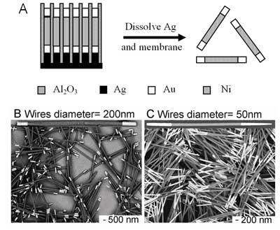 |
| (A) Schematic diagram of the strategy used to fabricate nanowires using electrodeposition in a nanoporous membrane. Scanning electron microscope (SEM) images of: (B) 200-nm and (C) 50-nm diameter Au–Ni–Au wires fabricated in nanoporous membranes. (The back scatter contrast is brightest for metals with higher atomic numbers; Au ends appears brighter than Ni.) (Source: Johns Hopkins University, Professor Gracias) |
| Professor David H. Gracias, the lead author of the study, told Nanowerk about their latest findings: |
| "There have been numerous ways developed to fabricate electrically functional nanowire building blocks. Strategies exist to use directed assembly to position these building blocks on microfabricated substrates to form functional nanoelectronic circuits." |
| Already, discrete functional nanoparticle-based electronic elements, e.g., resistors and diodes, can be fabricated in large numbers in a relatively cost-effective manner without the need for lithography. Therefore, in theory, it should be possible to fabricate functional electronic devices using metallic, semiconducting, and insulating multicomponent nanoparticles. |
| However, a major practical hurdle is the electronic integration of the nanoparticles with each other and with micropatterned substrates. |
| Gracias points out that, so far, the contact resistance between the nanowire and the substrate remained high and irreproducible. The precise positioning of the nanoparticles on the substrate is another hurdle. |
| Gracias says: "We have developed a way to bind nanowires to substrates to form reproducible contacts with low electrical resistance. Our strategy explores the use of nanoscale solder films to bind the nanoparticles to substrates." |
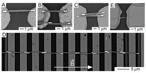 |
| Directed assembly of nanowires on top of patterned substrates using magnetic fields. The wires align between the pads in the direction of the field. By changing the concentration of the wire suspension the researchers could get: (A) a single wire, (B) two wires, and (C) many wires aligned between two Ni contact pads, or (D) many wires bridging several adjacent Ni contact lines. (E) Control sample with contact pads patterned on top of a nanowire. (Source: Johns Hopkins University, Professor Gracias) |
| "This is the first time that nanoscale solder has been shown to form a low resistance contact" he adds. "Several challenges such as reducing oxidation of the solder films and reducing diffusion were overcome in our work. |
| "We therefore were able to demonstrate a strategy to integrate nanowires and other nanoparticles with substrates to form functional nanoelectronic circuits." |
| The combined integration process of directed assembly and nanoscale soldering can be used in conjunction with other microfabrication processes to integrate functional nanoelectronic elements with substrates to generate integrated nanoelectronic devices. |
 By
Michael
Berger
– Michael is author of four books by the Royal Society of Chemistry:
Nano-Society: Pushing the Boundaries of Technology (2009),
Nanotechnology: The Future is Tiny (2016),
Nanoengineering: The Skills and Tools Making Technology Invisible (2019), and
Waste not! How Nanotechnologies Can Increase Efficiencies Throughout Society (2025)
Copyright ©
Nanowerk LLC
By
Michael
Berger
– Michael is author of four books by the Royal Society of Chemistry:
Nano-Society: Pushing the Boundaries of Technology (2009),
Nanotechnology: The Future is Tiny (2016),
Nanoengineering: The Skills and Tools Making Technology Invisible (2019), and
Waste not! How Nanotechnologies Can Increase Efficiencies Throughout Society (2025)
Copyright ©
Nanowerk LLC
|

Become a Spotlight guest author! Join our large and growing group of guest contributors. Have you just published a scientific paper or have other exciting developments to share with the nanotechnology community? Here is how to publish on nanowerk.com.
