| Posted: Feb 27, 2014 |
Conductive nanomaterials for printed electronics applications |
| (Nanowerk Spotlight) The term printed electronics refers to the application of printing technologies for the fabrication of electronic circuits and devices, increasingly on flexible plastic or paper substrates. Printed electronics has its origins in conductive patterns printed as part of conventional electronics, forming flexible keyboards, antennas and so on. Then came fully printed testers on batteries, electronic skin patches and other devices made entirely by printing, including batteries and displays (read more: "Printed electronics widens its scope"). |
| Traditionally, electronic devices are mainly manufactured by photolithography, vacuum deposition, and electroless plating processes. In contrast to these multistaged, expensive, and wasteful methods, inkjet printing offers a rapid and cheap way of printing electrical circuits with commodity inkjet printers and off-the-shelf materials. |
| All inkjet technologies are based on digitally controlled generation and ejection of drops of liquid inks using one of two different modes of operation: continuous and drop-on-demand printing. Conductive inkjet ink is a multi-component system that contains a conducting material in a liquid vehicle (aqueous or organic) and various additives (such as rheology and surface tension modifiers, humectants, binders and defoamers) that enable optimal performance of the whole system, including the printing device and the substrate. The conductive material may be dispersed nanoparticles, a dissolved organometallic compound, or a conductive polymer. |
| A review article in Small ("Conductive Nanomaterials for Printed Electronics") by Alexander Kamyshny and Shlomo Magdassi from The Hebrew University of Jerusalem, provides a state-of-the-art overview of the synthesis of metal nanoparticles; preparation of stable dispersions of metal nanoparticles, carbon nanotubes (CNTs) and graphene sheets; ink formulations based on these dispersions, sintering of metallic printed patterns for obtaining high electrical conductivity; and recent progress in the utilization of metal nanoparticles, carbon nanotubes, and graphene for the fabrication of various functional devices. |
| Requirements and challenges for printable dispersions of conductive nanomaterials |
| The use of nanomaterials for the formulation of conductive inkjet inks poses several challenges: |
|
|
| In their article, Kamyshny and Magdassi address these challenges in great detail and then go on to describe preparation methods for metal, graphene, and CNT-based inkjet inks, which are suitable for printed electronics, and post-printing processing methods for obtaining high electrical conductivities. |
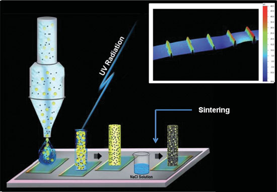 |
| Printing of a conductive 3D structure with the use of ink composed of an UV-curable emulsion and a dispersion of metal nanoparticles. Inset is a 3D profile of a 200 µm width lines composed of 1, 3, 6, 10, and 20 printed layers.(© The Royal Society of Chemistry) |
| Applications of conductive nanomaterials |
| The authors also discuss several applications of conductive nanomaterials for the fabrication of printed electronic devices. This includes fabrication and properties of transparent conductive electrodes, which are nowadays essential features for many optoelectronic devices, and inkjet-printed devices, such as RFID tags, light emitting devices, thin-film transistors (TFTs) and solar cells. |
| Transparent electrodes |
| The market for transparent electrodes has grown tremendously due to wide proliferation of LCD displays, touch screens, thin-film solar cells, and light emitting devices. The most widely used material is indium tin oxide (ITO) with a market share of more than 97% of transparent conducting coatings. ITO coatings have some major drawbacks, though, and many efforts to find alternatives are based on nanomaterials – metal nanoparticles, metal nanowires, carbon nanotubes, and graphene – which can be printed directly on various substrates without etching processes. |
| RFID tags |
| The main elements of an RFID (Radio Frequency Identification) tag are a silicon microchip and an antenna, which provide power to the tag and are responsible for communication with a reading device. Direct inkjet printing of antennas on plastic and paper substrates with the use of metal nanoparticles inks is a promising approach to the production of low-cost RFID tags. |
| Thin-film transistors |
| Conductive nanomaterials are used to produce the conductive features on both inorganic and organic TFTs. See for instance our recent Nanowerk Spotlight on inkjet printing of graphene for flexible electronics or the report on inkjet printing of single-crystal films of organic semiconductors. |
| Light-emitting devices |
| Light emitting devices (or electroluminescent devices, ELDs) are composed of a semiconductor layer placed between two electrodes, and emit light in response to electric current. LEDs to be used for lighting, require a highly conductive grid ('shunting lines') for homogeneous distribution of current around the lighting device. These circuits can be fabricated on various substrates including plastic, by various printing processes using conductive nanomaterials. |
| Solar cells |
| The first demonstration of inkjet-printed solar cells was already made in 2007 using fullerene-based ink. The results were discussed in this paper: "High Photovoltaic Performance of Inkjet Printed Polymer:Fullerene Blends". In recent years, metal nanoparticles as well as nanowires and CNTs have been also used in solar cells fabrication as well. |
| Concluding their review, the authors note that, in spite of the remarkable scientific progress in preparation processes and applications of conductive nanomaterials, they are still not widely used by the industry in significant quantities: "The current high price of commercially available inks, which are based mainly on the high cost silver, impedes their wide use for large area printed electronics. Therefore, research should be focused on the development of new nanomaterials and ink formulations based on low cost metals with high electrical conductivity such as copper, nickel, and aluminum." |
| They also note that in recent years, many scientific activities have been focusing on graphene and that we can expect future developments in printed electronics that will combine CNTs with graphene. Successive utilization of graphene for printed electronics requires ink formulations with high graphene loading, which are stable against flakes aggregation. |
| One final thought is the application of conductive nanomaterials in 3D printing of conductive patterns which opens some important perspectives for materials science. Although, this field is at its very early stages of research and development, and the search for new nanomaterials as well as suitable 3D fabrication tools based on wet deposition, it is a stimulating challenge for materials scientists. |
 By
Michael
Berger
– Michael is author of four books by the Royal Society of Chemistry:
Nano-Society: Pushing the Boundaries of Technology (2009),
Nanotechnology: The Future is Tiny (2016),
Nanoengineering: The Skills and Tools Making Technology Invisible (2019), and
Waste not! How Nanotechnologies Can Increase Efficiencies Throughout Society (2025)
Copyright ©
Nanowerk LLC
By
Michael
Berger
– Michael is author of four books by the Royal Society of Chemistry:
Nano-Society: Pushing the Boundaries of Technology (2009),
Nanotechnology: The Future is Tiny (2016),
Nanoengineering: The Skills and Tools Making Technology Invisible (2019), and
Waste not! How Nanotechnologies Can Increase Efficiencies Throughout Society (2025)
Copyright ©
Nanowerk LLC
|

Become a Spotlight guest author! Join our large and growing group of guest contributors. Have you just published a scientific paper or have other exciting developments to share with the nanotechnology community? Here is how to publish on nanowerk.com. |
