| Posted: Mar 15, 2006 |
In the future hydrogen economy, nanotech-based H2 sensors will be widely needed |
| (Nanowerk News) In the future hydrogen economy, hydrogen (H2) sensors will be a critical component for safety and widely needed. For example, H2 sensors will detect leaks from hydrogen-powered cars and fueling stations long before the gas becomes an explosive hazard. But even today a wide range of potential applications for H2 sensors exists, such as: |
| • Sensing H2 buildups in lead acid storage cells found in most vehicles. |
| • Detecting H2 leaks during petrochemical applications where high pressure H2 is used. |
| • Detecting impending transformer failure in electric power plants. |
| • Monitoring H2 buildup in radioactive waste tanks and in plutonium reprocessing. |
| In general, metal nanostructured materials, such as nanoparticles, nanowires and nanoarrays have attracted much attention due to their extraordinary electronic, optical and chemical properties. Palladium (Pd) nanowires receive a lot of attention from researchers as an ideal material for H2 sensing because Pd selectively absorbs H2 gas. |
| Compared with traditional, macroscopic, hydrogen sensors, Pd nanowire sensors operates via a totally different mechanism. In conventional sensors, H2 is detected when it adsorbs to a palladium wire, boosting the wire's electrical resistance. By contrast, H2 absorption lowers the nanowire's resistance by changing the wire's structure. When palladium absorbs H2, a new phase (a palladium hydride) is produced, causing the metal lattice to expand. As a result, the palladium grains swell, closing nanoscopic gaps present in the wires. This, in turn, allows more current to pass through the wire. |
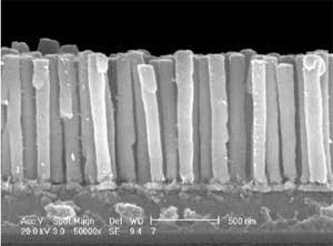 |
| SEM image of Pd nanowires standing freely on silicon substrate after removing the AAO template (Source: Sungkyunkwan University; reprinted with permission from Elsevier) |
| Scientists are continually looking to find faster, more efficient and more effective ways of building Pd nanowire arrays with potential use in H2 sensors. So far, Pd nanowires grown on graphite surface have been applied to fabricate a very sensitive H2 sensor. Now, researchers at Sungkyunkwan University in South Korea just reported for the first time the fabrication of free-standing Pd nanowire arrays on silicon substrate. |
| Sung M. Cho, one of the researchers, told Nanowerk: "Free-standing Pd nanowire arrays on silicon substrate have not yet been reported so far. In our study, Pd nanowire arrays have been successfully obtained by pulse electrodeposition using an anodized aluminum oxide (AAO) nanotemplate. The prepared Pd nanowire arrays are standing freely on the substrate and therefore could be used as a sensing element for a hydrogen sensor." |
| The "template method" is the simplest and most versatile approach for preparing metal nanowire arrays since it does not utilize expensive and sophisticated lithographic processes for defining nanoscale structures. It has been widely accepted that the AAO template is an ideal template because it possesses many desirable characteristics, including tunable pore dimensions, good mechanical strength and thermal stability. Besides, especially for metal nanowires, the AAO template method using electrodeposition has proved to be a cheap and high yield technique for producing large arrays of nanowires. |
| The free-standing Pd nanowires obtained in Dr. Cho's study are self-supporting and are standing up vertically to the substrate surface (a titanium-coated silicon wafer). They are uniform, independent and parallel to each other. These nanowires have a length of about 0.8 µm and a diameter of 80 nm with the aspect ratio of about 10. Pd nanowires arrays have been grown uniformly by this method in a relatively large area of about 5 cm². |
| The research paper, titled "Pulsed electrodeposition of palladium nanowire arrays using AAO template" will be published in the April 10, 2006 edition of Materials Chemistry and Physics. |
 By
Michael
Berger
– Michael is author of four books by the Royal Society of Chemistry:
Nano-Society: Pushing the Boundaries of Technology (2009),
Nanotechnology: The Future is Tiny (2016),
Nanoengineering: The Skills and Tools Making Technology Invisible (2019), and
Waste not! How Nanotechnologies Can Increase Efficiencies Throughout Society (2025)
Copyright ©
Nanowerk LLC
By
Michael
Berger
– Michael is author of four books by the Royal Society of Chemistry:
Nano-Society: Pushing the Boundaries of Technology (2009),
Nanotechnology: The Future is Tiny (2016),
Nanoengineering: The Skills and Tools Making Technology Invisible (2019), and
Waste not! How Nanotechnologies Can Increase Efficiencies Throughout Society (2025)
Copyright ©
Nanowerk LLC
|

Become a Spotlight guest author! Join our large and growing group of guest contributors. Have you just published a scientific paper or have other exciting developments to share with the nanotechnology community? Here is how to publish on nanowerk.com.
