| Posted: Jan 10, 2008 |
Electromechanical nanotechnology switches as alternatives to transistors |
| (Nanowerk Spotlight) A memory chip is an integrated circuit made of millions of transistors and capacitors. In the most common form of computer memory, dynamic random access memory (DRAM), a transistor and a capacitor are paired to create one memory cell, which represents a single bit of data. The capacitor holds the bit of information, either a 0 or a 1. The transistor acts as a switch that lets the control circuitry on the memory chip read the capacitor or change its state. Because each bit stored in a chip is controlled by one transistor, memory capacities tend to expand at the same pace as the number of transistors per chip - which still follows Moore's Law and therefore currently doubles every 18 months. |
| The problem is that the capacitor - consisting of two charged layers separated by an insulator - can shrink only so far. The thinner insulators get the more they allow charges to tunnel through. Tunneling increases the leakage current, and therefore the standby power consumption. Eventually the insulator will break down. |
| Researchers have been trying to develop electromechanically driven switches that can be made small enough to be an alternative to transistor-switched silicon-based memory. Electromechanical devices are suitable for memory applications because of their excellent ON–OFF ratios and fast switching characteristics. With a mechanical switch there is physical separation of the switch from the capacitor. This makes the data leakage problem much less severe. |
| Unfortunately they involve larger cells and more complex fabrication processes than silicon-based arrangements and therefore have not been so far an alternative to scaling down beyond semiconductor transistors. Researchers now have reported a novel nanoelectromechanical (NEM) switched capacitor structure based on vertically aligned multiwalled carbon nanotubes (CNTs) in which the mechanical movement of a nanotube relative to a carbon nanotube based capacitor defines ON and OFF states. |
| While nanoelectromechanical devices based on CNTs have been reported previously, so far it has not been possible to control the number and spatial location of nanotubes over large areas with the precision needed for the production of integrated circuits. |
| "We have demonstrated a viable structure and fabrication process for a NEM memory cell for ultra-large-scale integrated memory applications" Dr. Gehan Amaratunga tells Nanowerk. "The proposed write–read scheme is similar to that of a conventional DRAM, so conventional sensing schemes and CMOS (complementary metal-oxide semiconductor) circuits could be used, while taking advantage of the vertical nature of the NEM capacitor structure to achieve high integration densities." |
| Amaratunga is a Professor of Electrical Engineering and the head of the Electronics, Power and Energy Conversion (EPEC) Research Group within the Electrical Engineering Division of the Cambridge University Engineering Department in the UK. Working with an international group of collaborators from the Samsung Advanced Institute of Technology, and the Center for Nanotubes and Nanostructured Composites, SKKU Advanced Institute of Nanotechnology, both in South Korea, and the Microelectronics Research Centre, Cavendish Laboratory, at the University of Cambridge, he was able to demonstrate that one can make a vertically oriented switch on the nanoscale which works through the conversion of electrostatic force to mechanical movement. |
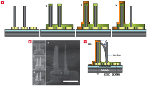 |
| A NEM switch based on vertically aligned multiwalled carbon nanotubes. Schematic diagram (a) and scanning electron micrographs (b) showing the fabrication process (see main text and Methods). Source S is connected to ground, and the drain D and gate G are connected to the bit line an the word line, respectively, to receive electrical signals. The substrate is Si and the insulating layer is SiO2 (300 nm thick). Nb is used for the source, drain and gate electrodes and access lines. The nanotube (gray) in the capacitor (on the left) has diameter ∼60 nm, the dielectric layer (green) is ∼40 nm thick, and the metal layer (orange) is ∼30 nm thick. The diameter of the capacitor structure is 200 nm and the scale bar in the micrograph corresponds to 500 nm. c, When positive bias voltages are applied to the drain and gate, electrostatic forces act to deflect the nanotube on the drain to make contact with the top metal of the capacitor on the source, causing it become charged. On removal of the gate bias voltage, if the combined electrostatic and van der Waals forces acting on the drain nanotube are weaker than the elastostatic force pulling it to the vertical, it will spring back to its original position, as shown in b, IV, leaving the nanoscale capacitor on the source in a charged state. (Reprinted with permission from Nature Publishing Group) |
| Amaratunga explains that the switching elements are formed by precision grown (diameter, height and spacial location) multiwalled carbon nanotubes (MWCNT). "By also fabricating a capacitor on one of the vertically oriented MWCNTs, we have demonstrated that it is also possible to achieve charging of a nanoscale capacitor through electromechanical switching and contact of vertically aligned MWCNTs" he says. "Such charge storage through switching is at the core of electronic memory – charged capacitor represents binary data '1' and uncharged binary data '0'. |
| These results have been reported in a recent paper in the December 23, 2007 online edition of Nature Nanotechnology ("Nanoscale memory cell based on a nanoelectromechanical switched capacitor"). |
| The key finding from this work is the demonstration that an electromechanically driven switch can be made small enough to be an alternative to transistor switched memory. This work can also be used to devise other types of memory cells (PROM, EEPROM etc.) and for utltra-small switches in electronic circuits. |
| The device reported by Amaratunga and his colleagues differs in important ways from previous proposals for CNT-based memory in that a single growth step allows for deterministic height and population control with defined spatial positioning of the MWCNTs. |
| "Due to the three-terminal structure of our device, the bias between source and drain can be changed, allowing for more flexible electromechanical drive conditions as well as random access" says Amaratunga. "Furthermore, the mechanical switching approach means that the ultra-shallow n- or p-type junctions and thin-gate dielectrics associated with nanoscale silicon transistors are not required. This removes the requirement for the complicated processing steps, high material purity and low contamination levels associated with silicon-based DRAM cells." |
| The researchers are now working on integrating the sensing electronics for detecting the '1', '0' charge data underneath the NEM switch in the silicon substrate. This will be comprised of standard CMOS transistors circuits. |
 By
Michael
Berger
– Michael is author of four books by the Royal Society of Chemistry:
Nano-Society: Pushing the Boundaries of Technology (2009),
Nanotechnology: The Future is Tiny (2016),
Nanoengineering: The Skills and Tools Making Technology Invisible (2019), and
Waste not! How Nanotechnologies Can Increase Efficiencies Throughout Society (2025)
Copyright ©
Nanowerk LLC
By
Michael
Berger
– Michael is author of four books by the Royal Society of Chemistry:
Nano-Society: Pushing the Boundaries of Technology (2009),
Nanotechnology: The Future is Tiny (2016),
Nanoengineering: The Skills and Tools Making Technology Invisible (2019), and
Waste not! How Nanotechnologies Can Increase Efficiencies Throughout Society (2025)
Copyright ©
Nanowerk LLC
|

Become a Spotlight guest author! Join our large and growing group of guest contributors. Have you just published a scientific paper or have other exciting developments to share with the nanotechnology community? Here is how to publish on nanowerk.com.
