| Posted: Jan 22, 2008 |
Amplifying biomolecular signals with nanoscale field effect transistors |
| (Nanowerk Spotlight) Biosensors, which incorporate biological probes coupled to a transducer, have been developed during the last two decades for environmental, industrial, and biomedical diagnostics. Typically, signal sizes generated by biomolecular binding tend to be extremely small - this is the limiting factor in reaching high sensitivity for these sensors. |
| The application of nanotechnology to biosensor design and fabrication and therapy at the molecular and cellular level promises to revolutionize bio-diagnostics. By exploiting the large surface-to-volume ratio of nanowires, nanotubes, nanocrystals, nanocantilevers, or quantum dots, researchers were able to build sensors that can measure extremely faint, and otherwise undetectable, signals - for instance a change in electrical conductance - arising from biomolecular binding on the surface of these nanodevices. Highly sensitive nanoprobes and nanosensors have the potential for a wide variety of medical uses at the cellular level. |
| For instance, the potential for monitoring in vivo biological processes within single living cells, e.g. the capacity to sense individual chemical species in specific locations within a cell, will greatly improve our understanding of cellular function, thereby revolutionizing cell biology. One way of enhancing signal strength is on the sensor device itself and researchers have now demonstrated such an on-chip signal amplification using a standard protein on a nanoscale field effect transistor. |
| A field effect transistor (FET) is a type of transistor that relies on an electric field to control the shape and hence the conductivity of a 'channel' in a semiconductor material. In 2005 it was shown in a series of experiments that a silicon nanowire can be used as the source-drain channel in FETs ("Multiplexed electrical detection of cancer markers with nanowire sensor arrays"). |
| Essentially, the binding of the biomolecule to the receptor behaves as a field effect (it changes the surface charge profile and the surface potential). The conductance and the I-V characteristics of the nanowire can therefore be used to characterize biomolecular binding. |
| "These nanowire field-effect sensors show significant advantages of real-time, label-free and highly sensitive detection of a wide range of analytes, including proteins, nucleic acids, small molecules, and viruses in single-element or multiplexed formats" Dr. Raj Mohanty explains to Nanowerk. "In conventional FETs, lithographic methods are used to fabricate gates at the bottom, the top, or the side. These bottom-up approaches, however, have limitations arising from the lack of control in materials and fabrication engineering. In contrast, top-down methods of fabrication by e-beam lithography or submicron optical lithography enable scalable manufacturing." |
| Mohanty, an Associate Professor of Physics at Boston University, and his research group are developing nanomechanical biosensors with single molecule sensitivity or single cell specificity. In a recent paper in Applied Physics Letters ("Nanoscale field effect transistor for biomolecular signal amplification") Mohanty, who collaborated with Prof. Shyam Erramilli's group at BU, shows that characteristics of differential conductance dI/dV can be used for even higher sensitivity in the field effect due to biomolecular binding. |
| "We demonstrate that the differential conductance dI/dV characteristics of a silicon nanowire FET with width below 200 nm show strong dependence on gate voltage" says Mohanty. "We use the peak position of the dI/dV curve to characterize antibiotin detection with sub-ng/ml sensitivity by functionalizing the silicon nanowire surface with biotin. From this measurement, we can extract the dissociation constant of biotin-antibiotin binding to be 5.2x10⁻¹⁰ M, in good agreement with other measurements." |
| By functionalizing the silicon nanowire surface with biotin, the researchers show that the device can be used to characterize protein binding. |
| "We were able to show equivalence between the field effect created by the biomolecular binding and the reference gate voltage" says Mohanty. "This equivalence allows the characterization of ligand-receptor binding by determining the calibrated gate voltage dependence rather than measuring the more cumbersome concentration dependence." |
| Mohanty points out that there are two fundamental advantages to their technique: "Firstly, we apply a top-down fabrication process using electron-beam lithography or optical lithography; secondly, we employ a silicon-based device architecture. Both of these approaches enable large-scale manufacturing in contrast to many other nanotechnology and non-nanotechnology methods." |
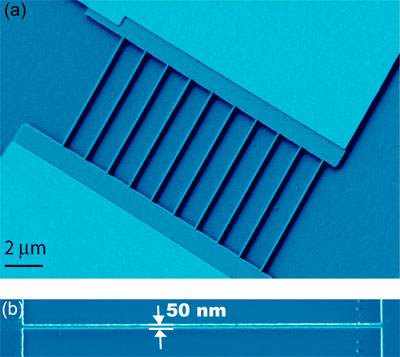 |
| a) Scanning electron micrograph of silicon nanowires, the working part of the biosensor. b) Top view of a 50 nm wide nanowire shows the controlled linear geometry (Image: Dr. Raj Mohanty, Boston University). |
| The scientists demonstrated their technique with a glucose sensor which they described in a separate paper, published on January 8, 2008 ("Silicon-based nanochannel glucose sensor"). This silicon nanochannel-based glucose biosensor technology offers the possibility of high density, high quality glucose biosensor integration with silicon-based circuitry. |
| Mohanty's team is now planning to come up with innovative techniques to further increase the signal or control the biomolecular binding locally. "In addition, we are working on integrating this device with microfabricated fluid channels for the handling of sample solutions" he says. |
 By
Michael
Berger
– Michael is author of four books by the Royal Society of Chemistry:
Nano-Society: Pushing the Boundaries of Technology (2009),
Nanotechnology: The Future is Tiny (2016),
Nanoengineering: The Skills and Tools Making Technology Invisible (2019), and
Waste not! How Nanotechnologies Can Increase Efficiencies Throughout Society (2025)
Copyright ©
Nanowerk LLC
By
Michael
Berger
– Michael is author of four books by the Royal Society of Chemistry:
Nano-Society: Pushing the Boundaries of Technology (2009),
Nanotechnology: The Future is Tiny (2016),
Nanoengineering: The Skills and Tools Making Technology Invisible (2019), and
Waste not! How Nanotechnologies Can Increase Efficiencies Throughout Society (2025)
Copyright ©
Nanowerk LLC
|

Become a Spotlight guest author! Join our large and growing group of guest contributors. Have you just published a scientific paper or have other exciting developments to share with the nanotechnology community? Here is how to publish on nanowerk.com.
