| Posted: Apr 14, 2006 |
A nanocapacitor with giant dielectric permittivity |
| (Nanowerk News) The area of nanodielectrics is relatively unexplored but research shows that nanocapacitors could find important applications for instance in energy storage and ultrasensitive transducers in nanoelectronic circuits. |
| The dielectric properties of nanomaterials has generated strong interests in the scientific community and nanomaterials having such properties are increasingly being referred to as "nanodielectrics". In general, a nanodielectric would consist of a single or multi-component dielectric possessing nanostructures, the presence of which results in the change of one or several of its dielectric properties. |
| "Surprisingly" says Dr. Shyamal Saha, "the area of nanodielectrics is relatively unexplored, despite the enormous scope of potential applications in power electronics and as gate electrodes in thin film transistors. Perhaps the greatest opportunity in nanodielectrics is in nanoparticulate materials." |
| Saha is with the Unit on Nanoscience at the Indian Association for the Cultivation of Science. In earlier work, he reported the observation of giant dielectric permittivity in an assembly of ultra fine silver metal particles as a result of quantum confinement of electronic wave functions. |
| "Nanoscale materials with this property of giant permittivity would be the ideal dielectrics for fabrication of a nanocapacitor, which is one of the fundamental components in nanoelectronic circuits" Saha says. |
| In a recent paper, titled "A nanocapacitor with giant dielectric permittivity" published on April 7, 2006 in the online edition of Nanotechnology, Saha and his collaborators describe a very simple technique to manipulate gold nanowires in between two microelectrodes to fabricate a nanocapacitor. This nanocapacitor shows an ultra high capacitance as a result of giant permittivity of the dielectric interface of the nanowires. Saha's co-authors are Manuel DaSilva and Timothy Sands from the School of Materials Engineering at Purdue University and Qingling Hang and David Janes from the School of Electrical and Computer Engineering, also at Purdue University. |
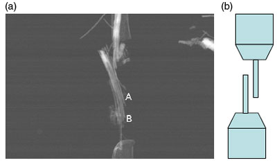 |
| (a) SEM micrograph of the nanowire device. The wire A from one electrode and the wire B from the other electrode form the nanocapacitor. (b) Schematic diagram of the nanocapacitor. (Reprinted with permission from the Institute of Physics Publishing ) |
| Saha explains to Nanowerk: "We believe the strong electrostatic force disrupts the loosely bounded surface atoms which are trapped at the dielectric interface between the nanowires. The presence of these isolated trapped gold metal atoms is the origin of this giant dielectic permittivity." |
| The researchers' experiment shows that the present nanocapacitor is ideal as it does not exhibit any frequency dispersion over the measured frequency range from several Hz to 1 MHz. However, the loss factor is high which should be minimized for application in nanoelectronic circuits. |
| According to Saha "the loss factor can be controlled by tailoring the thickness and number of atoms present in the interface and the resulting nanocapacitors could have application in energy storage, ultrasensitive transducers in nanoelectronic circuits, and also as high K materials in transistors." |
 By
Michael
Berger
– Michael is author of four books by the Royal Society of Chemistry:
Nano-Society: Pushing the Boundaries of Technology (2009),
Nanotechnology: The Future is Tiny (2016),
Nanoengineering: The Skills and Tools Making Technology Invisible (2019), and
Waste not! How Nanotechnologies Can Increase Efficiencies Throughout Society (2025)
Copyright ©
Nanowerk LLC
By
Michael
Berger
– Michael is author of four books by the Royal Society of Chemistry:
Nano-Society: Pushing the Boundaries of Technology (2009),
Nanotechnology: The Future is Tiny (2016),
Nanoengineering: The Skills and Tools Making Technology Invisible (2019), and
Waste not! How Nanotechnologies Can Increase Efficiencies Throughout Society (2025)
Copyright ©
Nanowerk LLC
|

Become a Spotlight guest author! Join our large and growing group of guest contributors. Have you just published a scientific paper or have other exciting developments to share with the nanotechnology community? Here is how to publish on nanowerk.com.
