| Posted: Jul 07, 2016 |
Room temperature cyclable healing of inorganic perovskite films |
| (Nanowerk Spotlight) A new kind of quantum dot system, inorganic halide perovskite quantum dots (IPQDs), have achieved widespread attention to both academia and industry in the past two years due to their excellent optical properties, such as high fluorescence quantum efficiency (up to 90%), emissions cover the entire visible region and narrow band emission (read more in our previous Nanowerk Spotlight: "Inorganic perovskite quantum dots for lighting and displays"). |
| Although developed only recently, inorganic halide perovskite quantum dot systems have exhibited comparable and even better performances than traditional quantum dots in many fields. They are expected to be applied in display and lighting technologies. |
| However, before we'll see widespread commercial applications there are a large number of basic problems to be studied. |
| Recently, a team of researchers from Nanjing University have reported an interesting cyclable surface dissolution and recrystallization phenomenon of inorganic perovskite crystals. This allows them to freely change size between nanometer and micrometer scales, and can be used to healing the defects inside perovskite films and hence improve the performances of optoelectronic devices. |
| This work, reported in the June 14, 2016 online edition of Advanced Functional Materials ("Healing All-Inorganic Perovskite Films via Recyclable Dissolution–Recyrstallization for Compact and Smooth Carrier Channels of Optoelectronic Devices with High Stability") should be useful for the understanding of perovskite and for improving the performances of perovskite devices, including solar cells, photodetectors, and LEDs. |
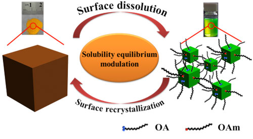 |
| Recyclable dissolution–recyrstallization (RDR) phenomenon of all-inorganic perovskite. Schematic of size evolution processes during washing and stirring. (Image: Institute of Optoelectronics & Nanomaterials, Nanjing University of Science and Technology) |
| "We report on a room temperature recyclable size evolution and micro-self-healing behaviors of inorganic halide perovskites, which result from the surface dissolution and recrystallization of inorganic perovskites with the effect of surfactants and polar solvents," Professor Haibo Zeng, Director of the Institute of Optoelectronics & Nanomaterials at Nanjing University of Science and Technology, tells Nanowerk. "These phenomena are intrinsic and universal for different perovskites prepared with different methods." |
| These findings can be applied to build compact and smooth carrier channels for optoelectronic devices via self-healing at room temperature. |
| Photodetectors based on the treated perovskite film exhibit improved response (>700%), external quantum efficiency (>700%), response speed (1 and 1.8 ms for rise and decay time), and stability, which are better than most of the planar perovskite photodetectors. |
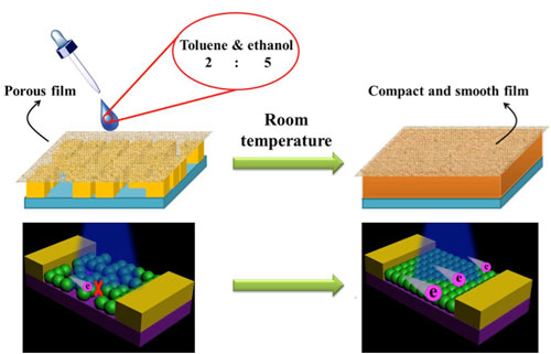 |
| Photoresponse of all-inorganic perovskite films before and after RDR healing. Schematic diagram of device structure of CsPbBr3 NCs before (left) and after (right) treating. (Image: Institute of Optoelectronics & Nanomaterials, Nanjing University of Science and Technology) |
| "Different from the classical Cd-based quantum dots, surfactants are not tightly bound to the surface of IPQDs, but highly dynamic," explains Zeng. "The surface diffusion coefficient reaches up to 166 µm2 s-1. When the surfactant disaffiliated from the surface of quantum dots, they will take away the surficial Cs+ and Pb2+ to maintain electrical neutrality, resulting in partial dissolution of the surface. Therefore, the size of the inorganic perovskite particles can be reversibly controlled between 10 nm-1 µm at room temperature under the influence of polar solvents and surfactant." |
| "Particularly" he points out, "on one hand, when purified with a mixed solvent of toluene and ethanol, the IPQDs will gradually become larger and eventually reach equilibrium because the dissolved ion composites connect small particles as solder. On the other hand, when large particles are stirred in toluene with surfactants, they will become smaller gradually and eventually reach equilibrium. The highly dynamic surfactants diffuse from the surface with cations, resulting in gradual surface dissolution." |
| According to these effects, the research team developed a room temperature film healing strategy for inorganic halide perovskites based on dissolution-recrystallization mechanism. |
| Low roughness and compact inorganic perovskite films can be obtained after simple solvent treatment. After treating, the films exhibit better optical response and carrier transport properties. |
| For example, compared to as-fabricated photodetectors, treated devices show improved response and detection and faster response speed. In addition, after continuous irradiation of high-intensity laser (442 nm) for 8 hours, there was only a decrease of 4.6% for photocurrent relative to the highest value while the untreated device shows a degradation of 34% after only 3.4 hours. |
| This work provides a new approach to improving the performance of devices based on inorganic halide perovskites and a comprehensive understanding of the surface structural and chemical features of inorganic halide perovskites. |
| "Our work would provide good reference for researchers since the developed film modification strategy is facile and suitable for all kinds of inorganic halide perovskite devices, especially for solution processed flexible devices," concludes Zeng. |
 By
Michael
Berger
– Michael is author of four books by the Royal Society of Chemistry:
Nano-Society: Pushing the Boundaries of Technology (2009),
Nanotechnology: The Future is Tiny (2016),
Nanoengineering: The Skills and Tools Making Technology Invisible (2019), and
Waste not! How Nanotechnologies Can Increase Efficiencies Throughout Society (2025)
Copyright ©
Nanowerk LLC
By
Michael
Berger
– Michael is author of four books by the Royal Society of Chemistry:
Nano-Society: Pushing the Boundaries of Technology (2009),
Nanotechnology: The Future is Tiny (2016),
Nanoengineering: The Skills and Tools Making Technology Invisible (2019), and
Waste not! How Nanotechnologies Can Increase Efficiencies Throughout Society (2025)
Copyright ©
Nanowerk LLC
|

Become a Spotlight guest author! Join our large and growing group of guest contributors. Have you just published a scientific paper or have other exciting developments to share with the nanotechnology community? Here is how to publish on nanowerk.com. |
