| Posted: Oct 06, 2016 |
3D printing highly conductive nanocomposites |
| (Nanowerk Spotlight) Carbon nanotube (CNT) enabled nanocomposites have received much attention as a highly attractive alternative to conventional composite materials due to their mechanical, electrical, thermal, barrier and chemical properties such as electrical conductivity, increased tensile strength, improved heat deflection temperature, or flame retardancy. |
| "Conventional methods used for forming conductive nanocomposites (CNCs) – such as solvent-casting, compression molding, or injection molding – usually require the utilization of molds while 3D printing methods build forms from a digitally designed 3D model," Daniel Therriault, a professor in the Laboratory for Multiscale Mechanics at Polytechnique Montreal, tells Nanowerk. "3D printing enables us to fabricate configuration with different structural parameters without the need to make a mold for each structure." |
| In new work, published in Small ("3D Printing of Highly Conductive Nanocomposites for the Functional Optimization of Liquid Sensors"), Therriault and his team report the fabrication of highly conductive carbon nanotube/polylactic acid (CNT/PLA) nanocomposites used as 3D printable conductive inks for fabrication of conductive scaffold structures applicable as liquid sensors. |
| The group is experienced in advanced 3D printing methods and they are developing 3D printing techniques in order to be able to print microstructures using various materials. In previous work, for instance, the team demonstrated the fabrication of various microstructures by a solvent-cast 3-D printing technique. |
| Conductive nanocomposites are one of the most promising materials in the field of electronics and sensors which motivated Therriault and his colleagues to get involved in the field. |
| This new work now shows how 3D printing can be used to explore experimentally the topology optimization of sensors where their sensitivity is related to their structural parameters. |
| "We used 3D printing for the functional optimization of an electronic device where a conductive composite is required," explains Dr. Kambiz Chizari, a former post-doctoral fellow in Therriault's group, and the paper's first author. "Our study shows how to apply 3D printing in order to find out the most suitable structural parameters of an electronic device, such as liquid sensors, so that we can optimize the device's functionality. It can be extremely useful combined with topology optimization methods to test the validity and practicality of the results obtained in theory." |
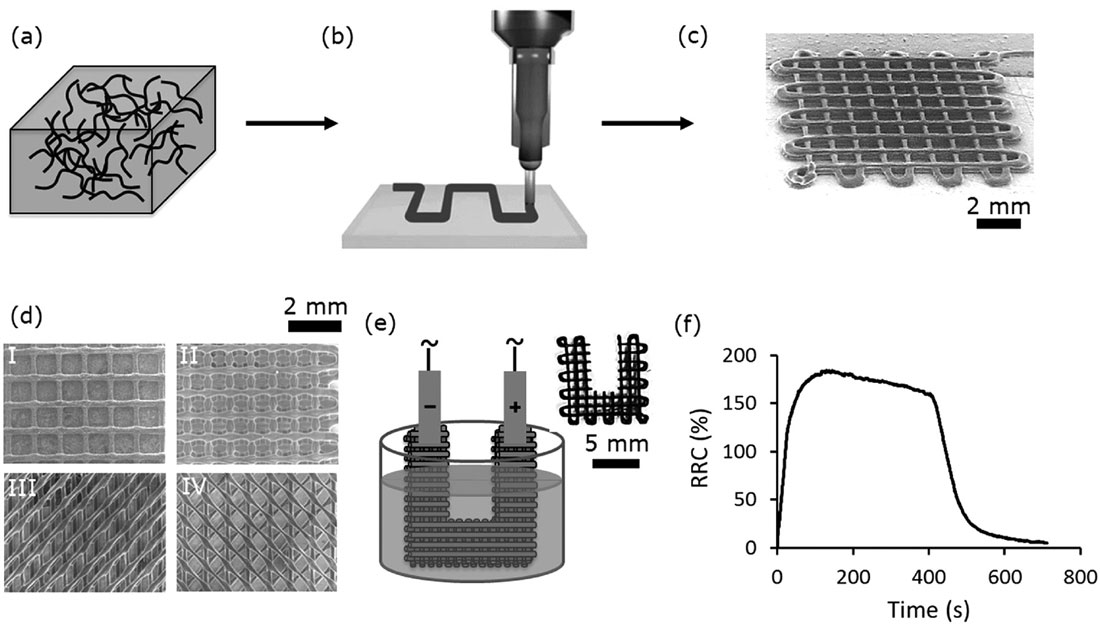 |
| Schematics and SEM images showing the fabrication, configurations, and liquid sensitivity tests of conductive scaffold structures. a) Schematic of CNT/PLA composites fabricated via ball mill mixing method. b) Schematics of 3D printing method used for fabrication of CNT/PLA scaffold structures. c) SEM image of a scaffold printed in two layers using the 3D printing method. d) Top view of SEM images of scaffolds printed in four layers with different patterns. I: Open window, II: closed window, III: zigzag I, and IV: zigzag II. e) Schematic showing liquid sensitivity testing of U-shaped cut scaffold. The immersion/drying cycles were 120/600 s. The inset shows a top view optical image of a U-shaped cut scaffold. f) A typical liquid sensitivity test graph showing the increase and decrease of the RRC of a liquid sensor while immersion/drying cycles. This test was on a scaffold with IFS of ∼0.7, thickness of ∼0.4 mm, and filament diameter of ∼231 µm printed in open window pattern. (Reprinted with permission by Wiley-VCH Verlag) (click on image to enlarge) |
| The team fabricated conductive polymer based 3D printable ink with conductivity as high as ~2350 S m-1, which appears to be the highest among other 3D printed polymer composites. |
| This technique can be very useful for the researchers in the field of 3D printing of conductive structures working on their different applications such as in the fields of electronics (e.g., 3D structured circuits), EMI shielding, various types of sensors (e.g., gas or strain sensors), etc. |
| Going forward, the researchers will investigate the mechanical properties of the printed structures. This factor is important for different applications of the 3D printed configurations where mechanical strength is required. |
| 3D printing at the nanoscale could be also highly useful especially in the field of electronics for printing of different electronic nanocomponents. Moving this process from the micro- to the nanoscale will not be a trivial challenge, though. |
| "We will also study the influence of different parameters such as the viscosity of the printing inks on the quality of the printing object in order to improve our solvent-cast 3D printing system," elaborates Therriault. "We are also involved in printing other types of materials such as metals, piezoelectric materials, short-fiber reinforced composites, etc." |
| Other research avenues the team plans to explore is to push the boundaries of electrical conductivity in printable inks so they can print conductive structures, even in freeform fashion, with the electrical conductivities close to metals. Another area is to print structures made from various materials such as metals, semiconductors, and ceramics. |
 By
Michael
Berger
– Michael is author of four books by the Royal Society of Chemistry:
Nano-Society: Pushing the Boundaries of Technology (2009),
Nanotechnology: The Future is Tiny (2016),
Nanoengineering: The Skills and Tools Making Technology Invisible (2019), and
Waste not! How Nanotechnologies Can Increase Efficiencies Throughout Society (2025)
Copyright ©
Nanowerk LLC
By
Michael
Berger
– Michael is author of four books by the Royal Society of Chemistry:
Nano-Society: Pushing the Boundaries of Technology (2009),
Nanotechnology: The Future is Tiny (2016),
Nanoengineering: The Skills and Tools Making Technology Invisible (2019), and
Waste not! How Nanotechnologies Can Increase Efficiencies Throughout Society (2025)
Copyright ©
Nanowerk LLC
|

Become a Spotlight guest author! Join our large and growing group of guest contributors. Have you just published a scientific paper or have other exciting developments to share with the nanotechnology community? Here is how to publish on nanowerk.com. |
