| Posted: Jan 05, 2017 |
Combining catalytic and electrical contact edge-effects to engineer the transport properties of nanocontacts to nanowires |
| (Nanowerk Spotlight) With the emergence of one-dimensional (1-D) and two-dimensional (2-D) nanostructures as the future of electronic materials there is a pressing need to develop new electrical contact preparation techniques that can refine the traditional processes for nanotechnological devices. The future of semiconductor devices brings significant challenges as the dimensions of the device components have been reduced from three-dimensional (3-D) to 2-D, and now to 1-D. |
| This research team, led by Prof. Wilks at Swansea University, is pursuing methods to engineer quantum based electrical contact technology to address the needs of the semiconductor industry as it develops devices based on nanomaterials. |
| Electrical contacts are essential components for any electrical device and when a lack of control over the final properties is present designing and optimising the system is impossible. Through decades of experimental and theoretical study a degree of control has been developed through band engineering when selecting contacts to large-scale planar devices such as field effect transistors. |
| Before the advent of nanotechnology, semiconductor devices applied thin material layers to engineer interfaces and contacts, such as lasers using quantum wells, in which case the active layers could be considered two-dimensional in nature. |
| Now with the intense study of nanotubes, nanowires, nanorods, quantum wires, nanoribbons and many other materials the physics in some cases has been reduced to one dimension. |
| New technologies based on these materials are emerging such as chemical and biological sensors, quantum computing, energy harvesting, lasers, and environmental- and photon-detectors. However, reliably engineering electrical contacts to these nanomaterials is essential to allow the development of nanoscience into a real-world technology and bring about the profound advances to the electronics industry that Scientists and Engineers know are possible. |
| Traditional methods of engineering electrical contacts have been applied to nanomaterials but often neglect the nanoscale effects that nanoscientists have worked so hard to uncover. |
| At the current time, a design toolbox to fabricate electrical contacts of chosen properties to nanomaterials is not close and research is lagging behind our potential application of the materials. |
| The ability to define the contacts as Schottky or Ohmic with high or low resistance is complicated by the 2-D, 1-D or quasi 1-D nature of many nanomaterials and the restricted volume of material available for engineering. Traditional techniques to engineer the contact properties inevitably alter the nanomaterial properties because of the inherently large and exposed material surface. |
Advances to enable contact engineering |
| Nanotechnology has delivered new materials and new technology and will continue to expand over the coming decades. Much of the usefulness stems from effects that occur at the atomic- or nanoscale. The research presented here, investigated by Dr. Alex M. Lord and Prof. Steve Wilks at Swansea University, has developed a deep understanding of a unique effect at these length scales that occurs in nanowires and combines the synergistic relationship between metal nanocatalyst particles and nanowires. |
| The mechanism described below has the potential for complete determination of the electrical contact properties without altering the nanowire properties. |
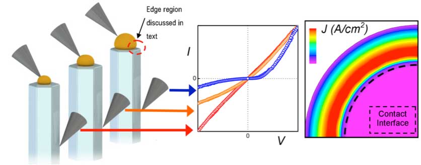 |
| Figure 1. Schematic diagram showing the electrical measurements performed on nanowires that have different sized Au particles (left) and the resultant current-voltage behaviour (centre) is controlled by geometrical effects that determine the magnitude of tunnelling current at the contact edge, shown by finite-element simulations (right). This effect is the basis for engineering the electrical contacts. (Image: Taken from Reference 1 that has a CC-BY licence) (click on image to enlarge) |
| We have recently shown that the electrical transport of nanocatalyst contacts on nanowires can be controlled by varying the size of the metal particle in relation to the nanowire diameter, Figure 1, due to quantum-mechanical tunnelling at the contact edge (Ref. 1: Nano Letters, "Controlling the electrical transport properties of nanocontacts to nanowires"). |
| This was confirmed in a newly-published study with UK collaborators Dr. Quentin Ramasse and Dr. Demie Kepaptsoglou at SuperSTEM, the EPSRC funded national facility for aberration-corrected STEM, UK, and also published in Nano Letters (Ref. 2: "Modifying the Interface Edge to Control the Electrical Transport Properties of Nanocontacts to Nanowires"), that developed a new experimental process (eSTEM) to directly correlate atomic-resolution electron microscopy to transport measurements on single Au-nanowire interfaces. |
| eSTEM allowed the authors to confirm the earlier result by adding or removing material to the tunnelling channel at the interface edge that enhances or removes the tunnelling path and to reveal a simple method for controlling the electrical transport properties of the nanocontacts, summarised in Figure 2. |
 |
| Figure 2. Atomically resolved evidence of a strong metal-support interaction (SMSI) at the Au-ZnO interface edge (left) creating Ohmic transport behaviour. Etching away the extraneous material eliminates the edge tunnelling path (right) producing defect-dominated transport through the bulk. (Image: Taken from Reference 2 that has a CC-BY licence) (click on image to enlarge) |
| Detailed atomic-resolution examination of Au-nanowire interfaces at SuperSTEM has shown that the ZnO nanowires and Au particles have interfaces that are structurally and chemically abrupt with high crystallographic quality. This feature ensures that the metal catalyst nanocontacts exhibit a dual effect at the interface edge in the region highlighted in Figure 1. |
| Firstly, accelerated chemical reactions take place at the edge region where the catalytic activity is greatest and secondly, tunnelling current is concentrated in the same region creating transport properties that are very surface sensitive, Figure 3. |
| There is a natural cross over between catalysts and electrical contacts because the behaviour of both can be heavily influenced by the surface properties of the material at the edge of the interface between the particle and support, as shown in Figure 3. |
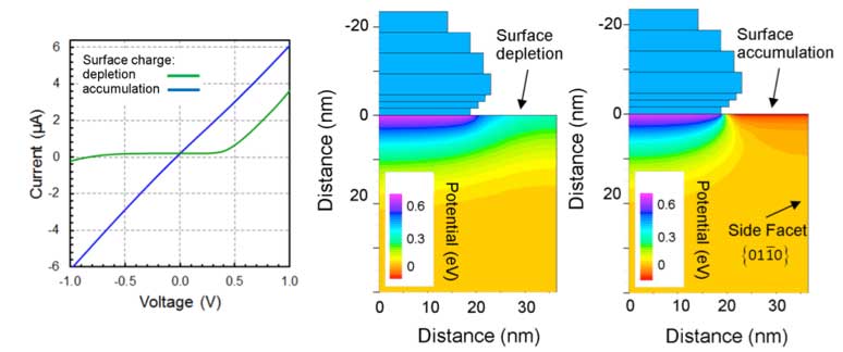 |
| Figure 3. I-V characteristics of Au nanocatalysts on ZnO Nanowires calculated with finite-element simulations when the ZnO surface near the contact edge is electron depleted or accumulated. This shows that chemical or structural modifications of the nanowire surface control the transport properties. (Image: Taken from Reference 1 that has a CC-BY licence) (click on image to enlarge) |
| The multifunctional capabilities of these nanocatalyst nanocontacts can provide great benefits when they are applied to new technological devices because catalysts can potentially bring huge increases of efficiency and surface sensitivity. Using simple methods such as modification of surface chemistry, or deposition techniques, the electrical properties of the contacts can be selected, Schottky or Ohmic, without any modification to the growth process, composition, or central interface quality. |
| These works show that by combining the catalytic effect of metal nanoparticles with quantum-transport effects when designing electrical contacts for nanomaterials real advances to next generation technologies can be realised. |
|
By Dr. Alex M. Lord, Centre for NanoHealth, Swansea University, UK
|

Become a Spotlight guest author! Join our large and growing group of guest contributors. Have you just published a scientific paper or have other exciting developments to share with the nanotechnology community? Here is how to publish on nanowerk.com. |
