| Posted: Feb 18, 2008 |
Wafer-level assembly of carbon nanotube networks |
| (Nanowerk Spotlight) Due to their exceptional electronic and mechanical properties, as well as their nanoscale size, carbon nanotubes (CNTs) could become the active electronic elements in addressing next generation electronic requirements for which silicon is not a solution. Already, it has been shown extensively that semiconducting CNTs can be made into electronic components such as transistors and switches (for instance, see our recent Spotlight "And you thought the iPod nano was small - here comes nanotechnology radio"). Their thermal, mechanical, chemical stability, and large current-carrying capacity make CNTs attractive for applications not only in in electrical interconnects but also field-effect transistors, cold cathode field emitters, and sensors. |
| Some of the problems in developing CNT-based electronic devices have to do with building reliable interconnections between CNTs and external electrical and mechanical systems and in developing a reliable fabrication batch process to allow for industrial-scale mass production that supports the direct manipulation and placement/growth of CNTs at specific locations. |
| Pointing to a possible solution, researchers now have demonstrated controllable and simultaneous wafer-scale assembly of CNT networks by dielectrophoresis. |
| "We have demonstrated wafer-scale assembly of CNT networks by dielectrophoresis (DEP)" Dr. Andrew Monica explains to Nanowerk. "We have successfully employed in situ monitoring of the CNT-DEP by measuring the current, voltage, and phase angle. The measured data allow for a correlation between the CNT network thickness and density, thus establishing the feasibility of a closed-loop system suitable for industrial applications." |
| Monica, a scientist at the Johns Hopkins University's Applied Physics Laboratory, is first author of a recent paper in Nanotechnology that describes a CNT-DEP technique that uses many lithographically patterned electrodes to assemble CNT networks on a wafer in a manner appropriate for massively parallel device fabrication ("Wafer-level assembly of carbon nanotube networks using dielectrophoresis"). |
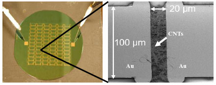 |
| Left: test substrate prior to CNT DEP; right: individual deposition site with CNTs assembled between the electrodes. (Reprinted with permission from IOP Publishing) |
| "Prior to our work we were unaware of any attempts to use in situ monitoring of the electrical characteristics of the CNT-DEP process" says Monica. "Combining this electrical monitoring of the process with corresponding chronological SEM images of the deposition revealed a correlation between the electrical behavior and the density of the assembled CNT network. Thus the potential exists to use the electrical characteristics of the deposition in a closed-loop industrial process to enable mass production." |
| Monica says that they also discovered that the electrode geometry and CNT suspension density play an intricate role with regards to network reproducibility across the wafer. While CNT-DEP can and has been used to assemble single-CNT devices, the reproducibility at the wafer level has been lacking so far. |
| The problem is that the electrodes are so small that the electric fields that attract the CNTs only sample a small volume of the suspension. Thus some deposition sites may see numerous CNTs while others will see few. To remedy this, the suspension density can be increased, but this often leads to CNTs forming bundles, thereby reducing the possibility for single-CNT device formation. So, unless the CNT density in the suspension can be increased significantly without a concomitant increase in CNT agglomeration, wafer-scale fabrication of CNT devices may be limited to those devices where the electrodes interact with a sufficiently large volume of suspension. |
| Monica and his collaborators examined CNT-DEP because it is a room-temperature, scalable process that can be done without the need for complicated systems or reactors. |
| "Recent efforts to use DEP for CNTs have primarily focused on electrode pairs or small arrays of electrodes onto which CNTs are deposited" says Monica. "The research demonstrates the deposition of individual CNTs between arrays of electrodes and the assembly of large-area CNT networks. These two approaches have different goals: parallel DEP assembly of single CNTs is aimed at high-performance logic or sensing devices, while large-area networks will likely be used for larger-area sensors or to exploit CNTs as a two-dimensional conducting film. Our work intended to demonstrate the practicality of manufacturing this latter class of devices." |
| The main problem so far with CNT-DEP has been the reproducibility issue at the wafer level. The ultimate goal would be to create a process where single CNTs can be deposited between electrodes across an entire wafer with a high yield. Currently, this goal has not been reached yet. |
| Monica points out that it is unknown if this is even possible since their results seem to point to a limitation on the minimal electrode geometry as well a constraints on the CNT suspension density. |
| Being able to assemble CNT networks by DEP at the wafer level, together with subsequent processing of the networks using standard lithography, etching, etc. could create a wide range of CNT-based devices. |
| "Our technique, at present, is still not suited for creating single-CNT devices, though numerous devices today employ bundles of CNTs" says Monica. "Our DEP technique with the appropriate processing would certainly be able to create similar CNT 'bundle' devices." |
| The researchers are now working towards refining the CNT-DEP process to ultimately produce single-CNT devices at the wafer level. However, as mentioned above, it is unknown if this will even be possible. Nevertheless, devices requiring bundles of CNTs could benefit greatly from these improvements to the CNT-DEP process. |
 By
Michael
Berger
– Michael is author of four books by the Royal Society of Chemistry:
Nano-Society: Pushing the Boundaries of Technology (2009),
Nanotechnology: The Future is Tiny (2016),
Nanoengineering: The Skills and Tools Making Technology Invisible (2019), and
Waste not! How Nanotechnologies Can Increase Efficiencies Throughout Society (2025)
Copyright ©
Nanowerk LLC
By
Michael
Berger
– Michael is author of four books by the Royal Society of Chemistry:
Nano-Society: Pushing the Boundaries of Technology (2009),
Nanotechnology: The Future is Tiny (2016),
Nanoengineering: The Skills and Tools Making Technology Invisible (2019), and
Waste not! How Nanotechnologies Can Increase Efficiencies Throughout Society (2025)
Copyright ©
Nanowerk LLC
|

Become a Spotlight guest author! Join our large and growing group of guest contributors. Have you just published a scientific paper or have other exciting developments to share with the nanotechnology community? Here is how to publish on nanowerk.com.
