| Posted: Jun 14, 2017 |
Current state of fabricating molecular electronics |
| (Nanowerk Spotlight) Since the genesis of the research field of molecular electronics, which is generally considered to have begun in 1974 with Aviram's and Ratner's early theoretical research ("Molecular rectifiers"), tremendous progress has been achieved both theoretically and experimentally by scientists and engineers who were fascinated by intriguing physical, chemical phenomena, and potential device applications of molecular junctions. |
| In a recent paper in ACS Nano ("High-Yield Functional Molecular Electronic Device"), scientists review recent experimental efforts for pursuing high-yield functional molecular devices, in which a bundle of molecules (the contacted molecules number more than ∼1000) is contained in a junction. |
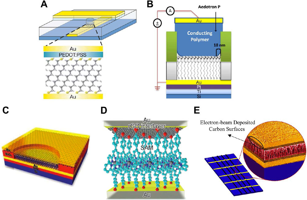 |
| Approaches for high-yield solid-state-based ensemble molecular junctions; conducting interlayer-based junctions. A) Conducting polymer PEDOT:PSS (© Nature). B) Conducting polymer Aedotron P (© ACS). C) Graphene (© Wiley). D) Reduced graphene oxide (© Wiley). E) Electron beam deposited carbon (© ACS). (click on image to enlarge) |
| The authors point out that several excellent reviews of the active field of nanoelectronics are available pertaining to single molecule junctions or ensemble molecular junctions (see for instance: "Molecular-Scale Electronics: From Concept to Function"). |
| In contrast, the overarching aim of their review article is to provide an overview of diverse experimental efforts for realizing the practical devices of the ensemble molecular junctions apart from single molecule junctions, in which distinctive electrical features are observed with high device yield. |
| To do so, they first summarize in detail a number of different approaches for achieving high-yield ensemble molecular junctions and discuss the practical applicability and suitability as a reliable practical device platform. |
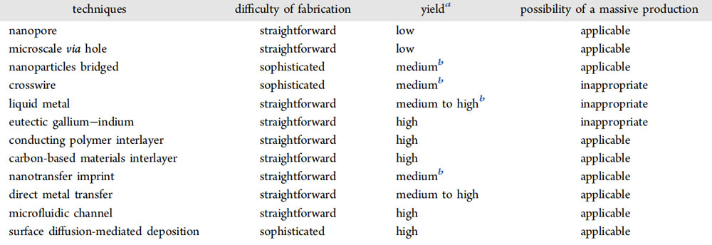 |
| Summary of fabrication techniques for ensemble molecular junctions. a: The standards of ranges of the device yield correspond to >70%, 20-70%, and <20% for high, medium, and low, respectively. b: The authors speculated the device yield by considering difficulty and addressability of each device fabrication method. (© ACS) (click on image to enlarge) |
| To provide a thorough review and comparison, they also mention traditional testbeds for the ensemble molecular junction, which usually lead to low device yield. |
| They then address primary advances in building functional molecular devices with desired functionalities based on the high-yield molecular junction platforms with programmed functional molecules. For example, they highlight the potential applications of molecular diodes, photoswitching devices, memory and optoelectronic devices. |
| With those functionalities, the authors discuss other considerations for real-life applications such as devices on flexible substrates and integration of the devices – aspects often neglected in previous reviews. |
| Finally, at the end of the review, they note the key issues critical to the success of the next-generation high-yield functional molecular device. |
| The researchers note that their overview aims to provide a better understanding of the current status of the rapid progress in the field of molecular electronics for the realization of commercially available functional molecular devices, which might be of crucial importance for the development of alternative electronics. |
 By
Michael
Berger
– Michael is author of four books by the Royal Society of Chemistry:
Nano-Society: Pushing the Boundaries of Technology (2009),
Nanotechnology: The Future is Tiny (2016),
Nanoengineering: The Skills and Tools Making Technology Invisible (2019), and
Waste not! How Nanotechnologies Can Increase Efficiencies Throughout Society (2025)
Copyright ©
Nanowerk LLC
By
Michael
Berger
– Michael is author of four books by the Royal Society of Chemistry:
Nano-Society: Pushing the Boundaries of Technology (2009),
Nanotechnology: The Future is Tiny (2016),
Nanoengineering: The Skills and Tools Making Technology Invisible (2019), and
Waste not! How Nanotechnologies Can Increase Efficiencies Throughout Society (2025)
Copyright ©
Nanowerk LLC
|

Become a Spotlight guest author! Join our large and growing group of guest contributors. Have you just published a scientific paper or have other exciting developments to share with the nanotechnology community? Here is how to publish on nanowerk.com. |
