| Posted: May 03, 2006 |
A new nanofabrication method to make polymer microlenses |
| (Nanowerk News) Researchers in Israel demonstrated a new technique for creating polymer microlenses. While current processes employed for manufacturing large microlens arrays are not compatible with the need to place single microlenses in very precise, strategic locations (such as an intersection of two nanochannels, for example) the Israeli group's method is specifically designed to do so. They deposit small drops of monomer solution with a nanopipette, mounted as an AFM probe (nano fountain pen, or NFP), and subsequently polymerize them, to yield microlenses. Their technique could ultimately lead to nano-biochips with integrated polymer optics. |
| Microlenses (with diameters of 4 µm and up) are widely used in consumer products such as flat panel displays or laser printers. Of great interest to researchers working on nano-biochips would be the capability to precisely position single microlenses: because the miniaturization of biochips would lead to a drastic reduction in the fluorescence signal that they emit, light collection efficiency is going to be crucial. Microlenses may provide a solution to this problem if they could be used to enhance the fluorescent signal. This would allow a further miniaturization of biochips, leading to a use of these arrayed biosensors to point-of-care clinical testing, environmental monitoring etc. |
| Dr. Levi Gheber and first author Mordechai Sokuler from the Department of Biotechnology Engineering at Ben-Gurion University of the Negev in Israel published their recent paper titled "Nano Fountain Pen Manufacture of Polymer Lenses for Nano-biochip Applications" in the March 18, 2006 online edition of Nano Letters. |
| "Our goal in manufacturing the microlenses this way is to have the ability to position them with very high precision, one by one, in strategic locations" Gheber explains to Nanowerk. "This ability is important in the context of future nano-biochips, which is a topic of interest in my lab, and that we have advanced in a number of ways." |
| "In previous work we showed that we can print proteins using NFP ("Protein printing with an atomic force sensing nanofountainpen") and active enzymes that specifically etch protein substrates" ("Nanolithography Using Protease Etching of Protein Surfaces" and "Manufacturing of Nanochannels with Controlled Dimensions Using Protease Nanolithography") Gheber says. |
| "In parallel, we are developing methods of integrating the optronics needed for reading fluorescence signals from future nano-biochips" he explains. "This is what led us to the development of this technique, and we also proved that such lenses can indeed collect light from fluorescent nano-spots with higher efficiency." |
|
|
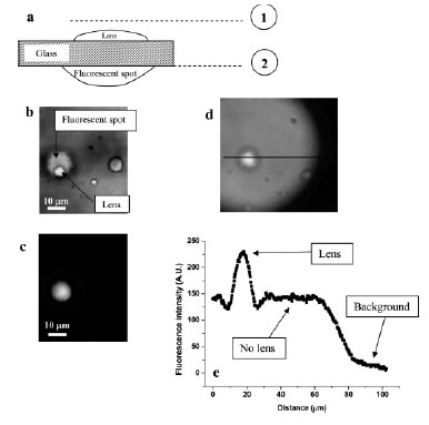 |
| (a) Schematic representation of the experimental setup: a fluorescent spot and a microlens are deposited on the opposite sides of a cover glass (170 µm thickness) with two different nanopipette. The focal plane of the microlens is labeled 1 and the plane of the fluorescent spot is labeled 2. (b) A bright-field image of the fluorescent spot and the lens taken in the focal plane of the lens, (1). (c) A fluorescence image of the fluorescent spot taken in its plane (2). (d) A fluorescence image taken in the focal plane of the lens (1). The round halo is the fluorescent light emitted by the fluorescent spot (in plane 2). The bright spot in the center of the halo is the image of the fluorescent spot concentrated by the microlens in its focal plane. (e) An intensity profile along the horizontal line in Figure d. The light intensity produced by the microlens is 1.5-fold higher than the light intensity detected directly from the fluorescent spot. (Reprinted with permission from ACS) |
| So far, Gheber and his group showed that they can control the focal length of these microlenses by changing one parameter only, which is the deposition time. While this is elegant, there are other parameters that can be used to control the radius of curvature of the lenses, and thus their focal length and consequently the numerical aperture. |
| "We are currently working on changing the wettability of the polymer-surface system" Gheber says. "In addition, we are looking into manufacturing waveguides using similar methods." |
 By
Michael
Berger
– Michael is author of four books by the Royal Society of Chemistry:
Nano-Society: Pushing the Boundaries of Technology (2009),
Nanotechnology: The Future is Tiny (2016),
Nanoengineering: The Skills and Tools Making Technology Invisible (2019), and
Waste not! How Nanotechnologies Can Increase Efficiencies Throughout Society (2025)
Copyright ©
Nanowerk LLC
By
Michael
Berger
– Michael is author of four books by the Royal Society of Chemistry:
Nano-Society: Pushing the Boundaries of Technology (2009),
Nanotechnology: The Future is Tiny (2016),
Nanoengineering: The Skills and Tools Making Technology Invisible (2019), and
Waste not! How Nanotechnologies Can Increase Efficiencies Throughout Society (2025)
Copyright ©
Nanowerk LLC
|

Become a Spotlight guest author! Join our large and growing group of guest contributors. Have you just published a scientific paper or have other exciting developments to share with the nanotechnology community? Here is how to publish on nanowerk.com.
