| Posted: Aug 01, 2017 |
Nanomanufacturing approach to rapidly optimize and fabricate quasi-random photonic nanostructures |
| (Nanowerk Spotlight) Quasi-periodic and random patterns in nature can exhibit extraordinary functions, such as iridescent color in bird wings, strong adhesion in gecko feet, and water repellency from lotus leaves. |
| At the nanoscale, quasi-random structures are being increasingly used for light management in solar cells and full-color displays. |
| The design and optimization of such photonic nanostructures, however, is very difficult and time consuming because thousands of geometric parameters must be tested one-by-one to achieve the desired performance. |
| Moreover, nature-inspired 3D nanostructures can be prohibitively expensive to make using modern nanoscale manufacturing processes. |
| Nanostructured surfaces with quasi-random geometries can manipulate light over a broad range of wavelengths and wide collection angles. Optimization and realization of stochastic patterns have typically relied on serial, direct-write fabrication methods combined with real-space design. |
| However, this approach is not suitable for customizable features or scalable nanomanufacturing. Moreover, trial-and-error processing cannot guarantee fabrication feasibility because processing-structure relations are not included in conventional designs. |
| New work by the Odom Group and the Chen Group, both at Northwestern University, shows a design approach integrated with scalable nanomanufacturing that can rapidly optimize and fabricate quasi-random photonic nanostructures. |
| A just published paper in Proceedings of the National Academy of Sciences ("Concurrent design of quasi-random photonic nanostructures") describes how the team employed wrinkle lithography integrated with concurrent design to produce quasi-random nanostructures in amorphous silicon at wafer scales that achieved over 160% light absorption enhancement from 800 to 1200 nm. |
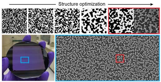 |
| Concurrent design-wrinkle nanolithography allows rapid prototyping of quasi-ordered photonic systems over wafer-scale areas and avoids the standard trial-and-error fabrication processes. (Image: Won-kyu Lee, Odom Group, Northwestern University) |
| "The quasi-periodicity of patterns, materials filling ratio, and feature depths could be independently controlled," Teri W. Odom, Charles E. and Emma H. Morrison Professor of Chemistry and Professor of Materials Science and Engineering at Northwestern University, tells Nanowerk. "We statistically represented the quasi-random patterns by Fourier spectral density functions (SDFs) that could bridge the processing-structure and structure-performance relations. Iterative search of the optimal structure via the SDF representation enabled concurrent design of nanostructures and processing." |
| The researchers fabricated 3D photonic nanostructures using concurrent design and manufacturing – that is, they carried out, simultaneously, the design of quasi-random nanostructures by machine-learning algorithms and the manufacturing of them by wrinkle lithography. |
| Wrinkle lithography is a new nanomanufacturing procedure that can transfer polymer wrinkle patterns into different materials to realize a nearly unlimited number of quasi-random nanostructures. Importantly, the complex geometries can be described computationally with only three parameters (instead of thousands typically required by other computational approaches), and these parameters have a one-to-one correspondence with structural processes in wrinkle lithography. |
| The team then used the digital designs of quasi-random nanostructures in an iterative search loop to determine the optimal nanowrinkles for a desired outcome; and as a proof-of-concept demonstration, they optimized quasi-random nanostructures in amorphous silicon and achieved enhancement in light absorption over the middle-wavelength range of the solar spectrum. |
| "Our methodology considers the actual (imperfect) fabrication conditions at the same time as the computational structure optimization," says Odom. "This concurrent design and processing of nanostructures paves the way to avoid trial-and-error nanomanufacturing and can increase the cost-effectiveness to prototype nanophotonic devices." |
| The researchers are currently considering other materials candidates such as polymers, metals, oxides, and emerging nanomaterials to integrate with their model for other customizable photonic applications, such as biological imaging and nanoscale random lasing. |
 By
Michael
Berger
– Michael is author of four books by the Royal Society of Chemistry:
Nano-Society: Pushing the Boundaries of Technology (2009),
Nanotechnology: The Future is Tiny (2016),
Nanoengineering: The Skills and Tools Making Technology Invisible (2019), and
Waste not! How Nanotechnologies Can Increase Efficiencies Throughout Society (2025)
Copyright ©
Nanowerk LLC
By
Michael
Berger
– Michael is author of four books by the Royal Society of Chemistry:
Nano-Society: Pushing the Boundaries of Technology (2009),
Nanotechnology: The Future is Tiny (2016),
Nanoengineering: The Skills and Tools Making Technology Invisible (2019), and
Waste not! How Nanotechnologies Can Increase Efficiencies Throughout Society (2025)
Copyright ©
Nanowerk LLC
|

Become a Spotlight guest author! Join our large and growing group of guest contributors. Have you just published a scientific paper or have other exciting developments to share with the nanotechnology community? Here is how to publish on nanowerk.com. |
