| Posted: Sep 05, 2017 |
Perovskite-based flexible image sensor array (w/video) |
| (Nanowerk Spotlight) Perovskite materials have attracted great attention in the fields of optoelectronics due to their significant optoelectronic properties. So far, the applications of perovskite thin-films have been limited to solar cells because the required high-definition patterning for optoelectronic devices hadn't been achieved yet. |
| Now, though, researchers in Korea have realized a high-resolution spin-on-patterning (SoP) process for the fabrication of optoelectronic devices arrays such as image sensors. |
| "Unlike previous works, which can only pattern perovskite materials on metal, patterning perovskite materials on the electron and hole transport layer is possible by using our novel SoP method," Dae-Hyeong Kim, a professor at Seoul National University, tells Nanowerk. "We expect that our work could help develop perovskite optoelectronics such as perovskite cameras and displays." |
| The researchers reported their findings in Advanced Materials ("High-Resolution Spin-on-Patterning of Perovskite Thin Films for a Multiplexed Image Sensor Array"). |
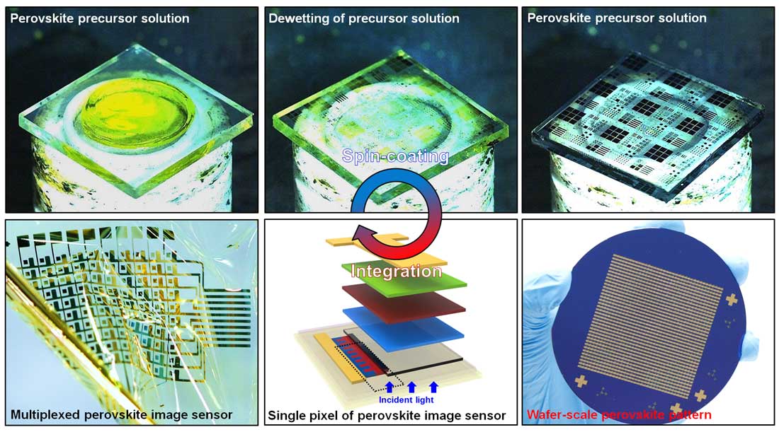 |
| Spin-on-patterning (SoP) of a inorganic–organic hybrid perovskite thin-film. Snapshot images at various states of the SoP process, captured from a slow-motion video, see below. (Image: Professor Dae-Hyeong Kim, Seoul National University) (click on image to enlarge) |
| Although there were similar research efforts on patterning organic/perovskite materials by manipulating the surface energy of metal oxide, patterning materials during spin-coating is difficult to realize. |
| In order to solve this problem, Kim's team observed and analyzed the intermediate steps of patterning perovskite with fast-speed cameras and subsequently optimized their SoP process. |
| Briefly, a densely packed hydrophobic self-assembled monolayer (SAM) is deposited on the hydrophilic oxide substrate. The photoresist is spin-coated and patterned. The photoresist-patterned oxide substrate is then treated with oxygen plasma using a reactive ion etcher to remove the SAM selectively, expose the oxide, and make that region hydrophilic. The removal of the photoresist leads to a patterned substrate with different surface energies (hydrophilic oxide region and hydrophobic SAM-modified region). Then, iii) the solution of perovskite precursors is spin-coated, which forms a thin solution film. Finally, the patterned solid-state perovskite film is obtained by thermal annealing. |
| The following video shows the detailed process: |
| The team notes that their SoP process is compatible with almost every spin-coated perovskite material and deposition technique (e.g., mixed-precursor, two-step, hot-casting, and solvent-engineering) as well as microfabrication processes used in the industry for mass production of multiplexed image sensor arrays. As such it can be applied to high-performance, ultrathin, and deformable optoelectronic device arrays. |
| As a demonstration, they integrated the patterned perovskite photodiodes (photodetecting unit) with silicon nanomembrane blocking diodes (active electronics) to build a multiplexed, ultrathin, lightweight, and deformable perovskite-on-silicon image sensor array. |
| However, large-scale fabrication with uniform pattern is crucial to commercializing perovskite optoelectronics. Although the researchers showed that wafer-scale fabrication is possible by using the SoP process, uniform patterns are not achieved (because the uniformity of the spin-coating process decreases with the increase of the number of pixels in the array). This problem will be addressed by future work. |
 By
Michael
Berger
– Michael is author of four books by the Royal Society of Chemistry:
Nano-Society: Pushing the Boundaries of Technology (2009),
Nanotechnology: The Future is Tiny (2016),
Nanoengineering: The Skills and Tools Making Technology Invisible (2019), and
Waste not! How Nanotechnologies Can Increase Efficiencies Throughout Society (2025)
Copyright ©
Nanowerk LLC
By
Michael
Berger
– Michael is author of four books by the Royal Society of Chemistry:
Nano-Society: Pushing the Boundaries of Technology (2009),
Nanotechnology: The Future is Tiny (2016),
Nanoengineering: The Skills and Tools Making Technology Invisible (2019), and
Waste not! How Nanotechnologies Can Increase Efficiencies Throughout Society (2025)
Copyright ©
Nanowerk LLC
|

Become a Spotlight guest author! Join our large and growing group of guest contributors. Have you just published a scientific paper or have other exciting developments to share with the nanotechnology community? Here is how to publish on nanowerk.com. |
