| Posted: Oct 04, 2017 |
Combining scanning probe technologies with microbeads for low-cost, high-resolution optical lithography systems |
| (Nanowerk Spotlight) Conventional optical lithography is the standard and most common technique in the semiconductor industry and in the microfabrication research field. Although several approaches have recently been developed to increase the resolution of optical lithography, most of the ultrahigh-resolution techniques are quite expensive. |
| In the past decade, there has been a growing interest in plasmonic nanostructures as starting point for several applications, ranging from optical biosensors to metasurfaces, from optical tweezers to nanolasers. In these cases, a low-cost optical lithography system with high spatial resolution would be of great interest to create prototypes of any desired structure. It would improve the testing process to focus the work on a proper design, saving time and money. |
| Among the important parameters in optical lithography is the spatial resolution you can get and the time you need to draw your pattern. Systems with regular and fixed patterns can be extremely fast but those systems are based on masks. Mask production is a time consuming and expensive process. |
| So-called mask-less systems can draw unorganized patterns directly on substrates, at the cost of longer process times. |
| All the lithographic instruments have a cost-dependent spatial resolution. By increasing the resolution, the costs can rise enormously. |
| Researchers at the Italian Institute of Technology (IIT) now have presented a new lithographic approach with a high-resolution, low-cost technique based on nanosphere lithography. They reported their findings in ACS Applied Materials & Interfaces ("Scanning Probe Photonic Nanojet Lithography"). |
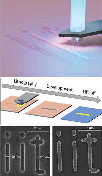 |
| (Top) Schematic illustration of a cantilever with a bead placed inside the circular rim. The bead is in contact with a substrate and shined with a beam. The cantilever is writing the Istituto Italiano di Tecnologia (IIT) logo that appears inside the substrate. (Middle) A schematic illustration of the workflow, on the right it is depicted the cantilever while is writing a line on the resist, then the exposed resist is removed during a development step, the work ends after a coating step with a lift-off process. (Bottom-left) SEM image of the IIT logo created with free writing lithography. The spatial resolution is below the incoming wavelength (405nm). (Bottom-right) SEM image of the IIT logo after metal deposition and lift-off. (Image: Italian Institute of Technology) |
| "Nanospheres are used for optical lithography as a consolidated method to achieve a sub-wavelength regular pattern with a cheap approach," Andrea Jacassi, a PhD in the Plasmon Nanotechnologies group at IIT and the paper's first author, tells Nanowerk. "Out technique improves this standard method, modifying an AFM cantilever to hold a single bead. These cantilevers are then used to achieve freehand lithography with a sub-wavelength resolution." |
| The team points out that their novel system can compete with commercial high-resolution standard instruments at a cost as much as one order of magnitude lower, opening the possibility to provide each laboratory with a high-resolution lithography instrument. According to them, this new technique has great potential to introduce rapid high-resolution microbead lithography as a new standard technique in laboratory environments due to its low cost. |
| "AFM systems are common instruments widespread in microscopy laboratories around the world," notes Jacassi. "With our method, a standard AFM can be easily upgraded to perform high-resolution optical lithography, reducing initial costs. Our method permits to use the AFM as a lithographic system or as a microscope simply by changing the cantilever." |
| Conventional microscopy is one of the widest and most used techniques in the lab, but it suffers from a fundamental limitation: it is impossible, with standard optics, to focus a free-propagating optical wave in the far-field with a spatial resolution below one-half of the incoming wavelength. |
| An approach that overcomes the diffraction limit of far-field optics with a simple and cheap solution is presented by photonic nanojets – an optical phenomenon that was discovered in 2004 ("Photonic nanojets open door to visible-light ultramicroscopy"). |
| The nanojet is a narrow, high-intensity electromagnetic beam that propagates from a plane-wave illuminated lossless dielectric microsphere with a diameter greater than the illuminating wavelength. It has already been shown that microspheres can offer low-cost and high throughput processes able to realize two-dimensional periodic arrays of deep sub-wavelength features, for instance enabling super-resolution biological microscopy. |
| These lithography approaches utilize a self-assembled planar array of microspheres as optical lenses, producing nanodisks at the bead focus spots where the high intensity enhancement generated by the nanojets is situated. |
| "What we have done is introduce a new idea to improve microsphere lithography," says Jacassi. "We modified a standard tipless cantilever by mounting a microbead on top of it. Then we coupled an AFM with a microscope and an UV laser. Moving the cantilever with the AFM, the nanojet can be used as a brush to write a desired pattern. This approach improves the previous lithographic methods by offering a new degree of freedom in pattern generation. In our system, the position between the bead and the resist is controlled and the pattern depends only on the mobility of the AFM probe." |
| The so modified AFM can produce lithographic patterns with high resolution and can be used to produce prototype of nanostructure thanks to the versatility in the pattern generation. |
| Jacassi recounts that this work has been a combination of ideas and technology needs. "We recently studied that nanojets produced using microbeads can be exploited for high-resolution microscopy. Integrating the microbead into the cantilever of an AFM system allows for enhancement of the optical performance of microscopes equipped with a low numerical aperture (NA) objective (Scientific Reports, Combination of scanning probe technology with photonic nanojets)." |
| "In fact" he continues, "microspheres embedded on cantilevers can act as portable high-NA nanolenses that are capable of extending the response of a low-NA objective to higher spatial frequencies. In a parallel activity, we were looking for a new lithographic technology that could produce free-hand patterns with high spatial resolution. Starting from the state-of-the-art of bead lithography and relying on the fact that we learned how to use a single bead embedded into a cantilever, we developed the new concept of a low-cost high-resolution mask-less lithography method." |
| To perform the microbead-assisted direct lithography it is necessary to place the bead in contact with the surface of the sample. Usually, in an AFM system the tip approach is controlled by a laser. In the case of the IIT team's work, the laser used in the cantilever positioning could degrade the lithography by exposing the photoresist. For this reason, the tip approach was carried out with a different method excluding the laser. |
| The cantilever, illuminated from below, exhibits interference fringes caused by a small deflection of the lever when the bead touches the sample. The researchers exploited the presence of those fringes as a method to guarantee the contact between the bead and the sample. |
| "The solution we found is a good alternative but it can slow down the workflow," says Jacassi. "This specific problem can be solved replacing the laser positioning method with a different one that doesn't interfere with the lithography process." |
| In order to create a versatile system able to perform both AFM microscopy and optical lithography, a more advanced pattern generator is needed. The IIT team plans to develop such improved software to increase the capabilities of this technique and for performing easily and rapidly any kind of unorganized patterns. |
| The method could also be used to expose 3D surfaces due to the capability of the AFM cantilever to follow the topography of a sample. This is particularly interesting because 3D high-resolution lithography is extremely complex and expensive using current lithographic standard systems based on objective focusing. |
| "A bead-embedded cantilever can be used directly in contact with the substrate without degradation of the lithography – such an approach is unobtainable with standard objectives that have a specific work distance and the positioning is a crucial and delicate procedure," concludes Jacassi. "With the bead-cantilever method, the AFM keeps its capability to scan the topography of a surface, opening the possibility to draw patterns on 3D surfaces. So far, such 3D high-resolution lithography has been obtained only with expensive and complex systems." |
 By
Michael
Berger
– Michael is author of four books by the Royal Society of Chemistry:
Nano-Society: Pushing the Boundaries of Technology (2009),
Nanotechnology: The Future is Tiny (2016),
Nanoengineering: The Skills and Tools Making Technology Invisible (2019), and
Waste not! How Nanotechnologies Can Increase Efficiencies Throughout Society (2025)
Copyright ©
Nanowerk LLC
By
Michael
Berger
– Michael is author of four books by the Royal Society of Chemistry:
Nano-Society: Pushing the Boundaries of Technology (2009),
Nanotechnology: The Future is Tiny (2016),
Nanoengineering: The Skills and Tools Making Technology Invisible (2019), and
Waste not! How Nanotechnologies Can Increase Efficiencies Throughout Society (2025)
Copyright ©
Nanowerk LLC
|

Become a Spotlight guest author! Join our large and growing group of guest contributors. Have you just published a scientific paper or have other exciting developments to share with the nanotechnology community? Here is how to publish on nanowerk.com. |
