| Posted: Oct 25, 2017 | |
Modular 'Lego' electronics |
|
| (Nanowerk Spotlight) Electronic systems are an assembly of various passive and active components forming a rigid structure and shape that make the whole system rigid and many a times bulky, which is a non-desirable trait for the many applications especially in wearable and implantable healthcare devices. | |
| Major challenges in assembly techniques for integration of microscale electronic devices are the yield and accuracy of the assembly tools like pick-and-place tools, and the usage of molten solder for surface tension driven assembly. However, high yields of >80% at device level will not guarantee a reliable system performance as individual component failure could result in a failure of the entire system. | |
| Researchers have now demonstrated a novel assembly technique for transforming traditional state-of-the-art complementary metal oxide semiconductor (CMOS) based integrated circuits (IC) and other electronic components into LEGO-like modules by providing unique geometrical identity to each module; and assembling these 'LEGO IC' without the need for bonding or soldering but with the highest yield, accuracy and throughput required to maintain a high system performance. | |
| "Our assembly technique is a unique method where we are capitalizing on commercially available IC and converting them into unique geometrical shapes for different modules," Muhammad Mustafa Hussain, an Associate Professor of Electrical Engineering at King Abdullah University of Science and Technology (KAUST), who led the work, tells Nanowerk. "Individual devices assembly is shown using similar approach, however, system level integration is not demonstrated due to fact that yields are not sufficient to illustrate the system performance." | |
| "Beside this" he adds, "the approach of having different geometrical identities to different IC not only gives aesthetic values to traditional bulky and rectangular IC but also help individual IC identification by means of non-microscopic observations like touch or sight." | |
| Hussain and his team have published their findings in Advanced Materials Technologies ("Modular Lego-electronics"). | |
 |
|
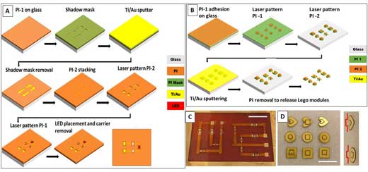
| Fabrication schematics for A) flexible binding site (inverse replica) of the Lego module on PI. B) flexible Lego module fabrication. C) Digital image of binding sites after fabrication on glass substrate before release, and D) digital image of Lego modules in three different shapes (heart, square, and circle) with same and different teeth. Bottom right shows the contour of the step height for Lego teeth. Scale bar is 5 mm. (© Wiley-VCH Verlag) (click on image to enlarge) | |
| The team points out that they achieved 100% yield with their tools with high accuracy and reliable identification and placement of modules. | |
| The next stage of this work will be the demonstration of a self-assembly process of these modular components. | |
| "Guiding the modules to their binding sites using fluidic agitation or surface tension driven approach for self-assembly which may eliminate the necessity of manual handling of individual modules as well as increasing overall throughput," notes Hussain. | |
| "Lego-like assembly of ICs will open up opportunities for high-throughput precision assembly in electronics manufacturing and biologically facilitated self-assembly of complex electronic system," he concludes. "Each of them brings additional requirement of understanding nature and exploring solutions using multi-disciplinary perspectives and resources. I won’t say they are challenging, rather exciting opportunities for all." | |
 By
Michael
Berger
– Michael is author of three books by the Royal Society of Chemistry:
Nano-Society: Pushing the Boundaries of Technology,
Nanotechnology: The Future is Tiny, and
Nanoengineering: The Skills and Tools Making Technology Invisible
Copyright ©
Nanowerk LLC
|
|
|
Become a Spotlight guest author! Join our large and growing group of guest contributors. Have you just published a scientific paper or have other exciting developments to share with the nanotechnology community? Here is how to publish on nanowerk.com. |
|
