| Posted: May 10, 2006 |
Lithographically defined self-assembled nanoparticle films |
| (Nanowerk News) Researchers at the University of New Mexico have demonstrated a new, simple, and facile approach to the fabrication of various nanopatterned films composed of nanoparticles. The findings could lead to nanoparticle sensors for both biological and chemical species. |
| There are many applications for mesoscopically organized nanoparticle films in areas such as electronics, photonics, sensors and catalysts. Self-assembly is a powerful technique for organizing nanoparticles with precise short-range order, but there are many applications requiring a long-range order and a range of geometries and length scales over which the particles are organized – ranging from single particles to macroscopic areas such as contact pads. Fabricating large-area mesoscopic patterns of nanoparticle films on flat surfaces with high quality and uniformity has remained a challenge. |
| In recent work Professor Steven R. J. Brueck, director of the Center For High Technology Materials at the University of New Mexico, and his group report a simple, inexpensive approach that combines bottom-up self assembly and top-down lithography to fabricate nanoparticle film patterns with submicrometer periodicity. |
| The group's paper, titled "An Approach to Lithographically Defined Self-Assembled Nanoparticle Films" appeared in the March 24, 2006 online edition of Advanced Materials. |
| Most previous work has proceeded by an additive process of first defining mesoscopic areas (lines, circles, interconnects, etc.) using a lithographic process and then attempting to fill these patterns with nanoparticles using any of a number of directed self-assembly approaches. |
| Brueck explained their new approach to Nanowerk: "In this work, we turned the process around and deposited a uniform layer of nanoparticles, which can be done easily over macroscopic dimensions, and then deposited, exposed and developed a layer of photoresist and used the developed resist as an etch mask to transfer the pattern into the nanoparticles. The end result is a much larger area of nanoparticle patterns with better pattern fidelity and with the flexibility to fabricate patterns with a larger range of sizes and complexity. " |
| There are four main steps in the fabrication process: spin-coating, interferometric lithography (IL), reactive-ion etching (RIE) and photoresist (PR) removal. |
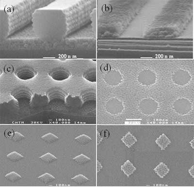 |
| SEM images showing lithographically defined patterned nanoparticle films with combination of spin-coating driven self-assembly of nanoparticles, interferometric lithography (IL) and reactive ion etching (RIE): (a) photoresist pattern above blanket nanoparticle layer; ( b) nanoparticle pattern after etching and photoresist removal; (c) photoresist pattern; (d) nanoparticle pattern after etching and photoresist removal; (e)-(f) 2D isolated discs. (Source: Deying Xia, S. R. J. Brueck, University of New Mexico) |
| "Since the film deposition occurs before patterning, alternative deposition methods such as electrostatic and convective self-assembly are also applicable for the film formation, which, of course, is not limited to silica nanoparticles" Brueck says. "In addition, the particles can be functionalized before fabrication, as long as a compatible etch and PR-removal process is used." |
| Brueck points out that integrated circuits incorporate many length scales from individual transistors, with ∼50-nm gate lengths, to cross-chip interconnects with ∼cm lengths. Similarly biology integrates multiple length scales to provide functionality that goes beyond that available at a single length scale. |
| "Our ability to engineer structures by self-assembly is primitive by comparison" he says. "This work is a small step towards combining top-down and bottom-up fabrication technologies to produce functional devices and systems enabling new capabilities." |
| In previous work ("Fabrication of enclosed nanochannels using silica nanoparticles"), Brueck and his group describe the use of related nanoparticle deposition techniques to fabricate nanochannel arrays with porous interconnections. These are unique structures combining multiple length scales in a facile way that will be very important for applications in bioseparations and in catalysis and other applications where it is necessary to deliver large fluid volumes to nanoscale objects and to maximize the cross section of exposure to the nanoparticles. |
| Two previous related papers by Brueck's group appeared in Advanced Materials ("Directed Self-Assembly of Silica Nanoparticles into Nanometer-Scale Patterned Surfaces Using Spin-Coating") and Nano Letters ("A Facile Approach to Directed Assembly of Patterns of Nanoparticles Using Interference Lithography and Spin Coating"). |
 By
Michael
Berger
– Michael is author of four books by the Royal Society of Chemistry:
Nano-Society: Pushing the Boundaries of Technology (2009),
Nanotechnology: The Future is Tiny (2016),
Nanoengineering: The Skills and Tools Making Technology Invisible (2019), and
Waste not! How Nanotechnologies Can Increase Efficiencies Throughout Society (2025)
Copyright ©
Nanowerk LLC
By
Michael
Berger
– Michael is author of four books by the Royal Society of Chemistry:
Nano-Society: Pushing the Boundaries of Technology (2009),
Nanotechnology: The Future is Tiny (2016),
Nanoengineering: The Skills and Tools Making Technology Invisible (2019), and
Waste not! How Nanotechnologies Can Increase Efficiencies Throughout Society (2025)
Copyright ©
Nanowerk LLC
|

Become a Spotlight guest author! Join our large and growing group of guest contributors. Have you just published a scientific paper or have other exciting developments to share with the nanotechnology community? Here is how to publish on nanowerk.com.
