| Posted: Apr 19, 2018 |
One-dimensional quantum materials can deliver record-high current densities |
| (Nanowerk Spotlight) The advent of graphene resulted in a massive, world-wide, effort directed at investigation of other two-dimensional (2D) layered materials. |
| The one-dimensional (1D) bundled materials have received considerably less attention. Similar to the 2D layered materials with covalently bonded layers separated by the van der Waals gaps, the 1D materials consist of covalently bonded one-dimensional wires with van der Waals gaps between the wires. |
| The term van der Waals gap refers to the weak binding force, which allows for the separation of the atomic plane in 2D materials and atomic chains in 1D materials. Due to their lower dimensionality, the 1D van der Waals materials exhibit even more fascinating quantum properties than their 2D counterparts. |
| Example of 1D van der Waals materials include transition metal trichalcogenides, which have strong covalent bonds in one direction and weaker bonds in cross-plane directions. They can be prepared as crystalline nanowires or nanoribbons consisting of 1D atomic threads, i.e. atomic chains. |
| A group of researchers led by Professor Alexander A. Balandin, University of California – Riverside discovered that quasi-1D ZrTe3 nanoribbons reveal an exceptionally high current density, on the order of ∼100 MA/cm2, at the peak of the stressing DC current. This level of the current density exceeds that in any conventional metals like copper by almost two orders of magnitude. |
| "Conventional metals are polycrystalline. They have grain boundaries and surface roughness, which scatter electrons. Quasi-one-dimensional materials such as TaSe3 or ZrTe3 consist of single-crystal atomic chains in one direction. They do not have grain boundaries and often have atomically smooth surfaces after exfoliation. We attributed the exceptionally high current density in ZrTe3 to the single-crystal nature of quasi-1D materials," explains Balandin. |
| The UC Riverside team used shadow mask method to prepare multiple devices for testing. The nanoribbons of ZrTe3 of nanometer scale cross-sections were interfaced with conventional metal contacts (see Figure 1). |
| Depending on the specific polymorph and the cross-sectional dimension ZrTe3 nanoribbons reveal metallic or semiconducting behavior opening up possibilities of applications in interconnects or electron device channels. The results of this investigation appear in IEEE Electron Device Letters ("Current Carrying Capacity of Quasi-1D ZrTe3 van der Waals Nanoribbons") . Adane Geremew, the first author of the paper, is a PhD student in Balandin’s group. Professor Tina Salguero, University of Georgia, synthesized bulk materials, which were used for exfoliation of nanoribbons. |
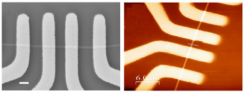 |
| Figure 1: Scanning electronic microscopy (SEM) image of a quasi-one-dimensional ZrTe3 nanoribbon device (left panel). Atomic force microscopy (AFM) image of another quasi-one-dimensional ZrTe3 nanoribbon device. AFM characterization was used to determine the nanowire width and thickness. (Image: Professor Alexander A. Balandin and Adane Geremew, University of California – Riverside) |
| The complementary metal-oxide semiconductor (CMOS) technology is the core enabler for all information technologies. As aggressive scaling in the CMOS technology continues, there is a growing need to examine new materials that can be used for nanometer-scale local interconnects or device channels. More than a decade ago, the electronic industry moved from aluminum to copper to lower resistance and improve reliability of interconnects via reduced electromigration. Projected downscaling to few-nanometer dimensions requires delivery of exceptionally high current densities. |
| In 2016, the UC Riverside team has reported that metallic TaSe3 nanowires have breakdown current density on the order of ∼10 MA/cm2. In principle, such quasi-1D materials could be downscaled by exfoliation, or grown directly, into nanowires with a cross-section of ∼1 nm × 1 nm, which corresponds to an individual atomic thread, i.e. chain. |
| In the present study, the level of the current sustained by the ZrTe3 quantum wires reached ∼100 MA/cm2 (see Figure 2). This current density is higher than what was reported for any metals or other 1D materials. It reaches the current density in carbon nanotubes and graphene. |
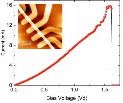 |
| Figure 2: High field current - voltage characteristics of the representative quasi-1D ZrTe3 nanoribbon device. The apparent breakdown current density, calculated with the AFM measured thickness and SEM measured width, corresponds to ∼108 A/cm2, i.e. 100 MA/cm2, reached at the voltage bias of ~1.6 V. (Image: Professor Alexander A. Balandin and Adane Geremew, University of California – Riverside) |
| "Our proof-of-concept experiments were conducted with the exfoliated material. However, the methods for a controlled growth of the quantum 1D materials, both metals and semiconductors, are already under development. This is important for practical applications," explains Balandin. "The most exciting thing about the quasi-1D materials is that they can be truly synthesized into the channels or interconnects with the ultimately small cross-section of one atomic thread – approximately one nanometer by one nanometer," he adds. |
| The work at UC Riverside was supported, in part, by the Semiconductor Research Corporation (SRC) contract: One-Dimensional Single-Crystal van-der-Waals Metals: Ultimately-Downscaled Interconnects with Exceptional Current-Carrying Capacity and Reliability. Materials synthesis and characterization in the University of Georgia and UC Riverside were supported, in part, by NSF through the Emerging Frontiers of Research Initiative (EFRI) 2-DARE award EFRI-1433395: Novel Switching Phenomena in Atomic MX2 Heterostructures for Multifunctional Applications. |
|
Provided by UC Riverside as a Nanowerk exclusive
|

Become a Spotlight guest author! Join our large and growing group of guest contributors. Have you just published a scientific paper or have other exciting developments to share with the nanotechnology community? Here is how to publish on nanowerk.com. |
