| Posted: Aug 14, 2018 |
Opto-thermoplasmonic patterning of 2D materials |
| (Nanowerk Spotlight) Traditional top-down patterning techniques – including photolithography, electron beam lithography, and ion beam lithography – have been employed to fabricate high-quality micro- and nanopatterns of diverse two-dimensional (2D) materials. However, these fabrication techniques typically require complex and expensive instruments and multiple-step processing. |
| An alternative approach is laser processing of 2D materials, which is a remotely controlled, one-step, maskless, and low-cost fabrication technique. The down-side to this process is the requirement for high optical power and the fact that the fabrication of sub-micrometer patterns is still challenging. |
| To overcome these problems, researchers have developed an all-optical lithographic technique called optothermoplasmonic nanolithography (OTNL) to achieve high-throughput, versatile, and maskless patterning of different atomic layers. |
| "Our motivation to develop this novel optical tool has been to achieve simple, low-power, high-throughput and precise patterning of 2D materials with all optical control," Dr. Linhan Lin, first author of a paper on this work (Advanced Functional Materials, "Optothermoplasmonic Nanolithography for On-Demand Patterning of 2D Materials"), tells Nanowerk. |
| Taking graphene and molybdenum disulfide (MoS2) monolayers as examples, the team at the University of Texas at Austin, led by professors Yuebing Zheng and Deji Akinwande, show that both thermal oxidation and sublimation in the light-directed temperature field can lead to direct etching of the atomic layers. |
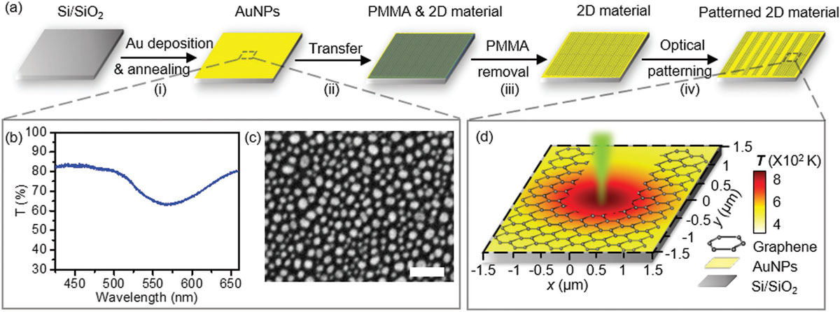 |
| General concept of OTNL. a) Schematic flowchart of OTNL process for 2D materials patterning, which includes i) fabrication of thermoplasmonic substrate; ii) transfer of 2D materials onto the thermoplasmonic substrate; iii) PMMA removal by acetone; and iv) optical patterning of 2D materials. b) Absorption spectrum and c) scanning electron micrograph of thermoplasmonic substrate. d) Enlarged scheme showing the working area of OTNL. The embedded shows the simulated temperature distribution of thermoplasmonic substrate around the laser spot. Laser beam size: 1 µm and incident power: 6.4 mW µm-2. (Reprinted with permission by Wiley-VCH Verlag) (click on image to enlarge) |
| They demonstrate the low-power (∼5 mW µm-2) and high-resolution (down to 300nm) patterning of both graphene and MoS2 monolayers through exploiting thermal oxidation and sublimation at the highly localized thermoplasmonic hotspots (which are created by plasmon-enhanced optical heating). |
| The researchers also discovered that gold (Au) nanoparticles can reduce the formation energy (∼0.6 eV) of carbon (C) monovacancies through bonding between undercoordinated C and Au, leading to a significant Au-catalyzed graphene oxidation and reducing the required operational optical power. |
| "The concept of opto-thermoplasmonic patterning can be widely applied in the laser processing of atomic-thin materials at different scales (10-9 to 10-3 m), which can be further explored for all-optical and precise morphologic control at quantum regions," says Jingang Li, the co-first author of the paper. |
| In this work, the team further demonstrates programmable patterning of 2D materials into complex and large-scale nanostructures by steering the laser beam. |
| There are several specific potential applications of the OTNL approach: |
|
|
| Movie shows the real-time patterning of a nanohole array in MoS2. (Video: Zheng Group, The University of Texas at Austin) |
| "The OTNL technique can be widely applied to fabricate different electronic and photonic devices based on 2D materials," Zheng concludes. "Compared to conventional lithographical methods, OTNL will provide a new way for simple, low-cost and large-scale fabrication of diverse patterns with arbitrary configurations. We can foresee various applications of OTNL in fabrication of ultrathin devices for photon detection, field-effect transistors, light emitting diodes, biosensors and so on." |
| Future research in optical patterning of 2D materials will focus on the improvement of patterning resolution to enable light-matter coupling at nanoscale. Potential challenges in this area include how to maintain the quality of 2D materials and how to dynamically control the nano-heaters optically and precisely. |
 By
Michael
Berger
– Michael is author of four books by the Royal Society of Chemistry:
Nano-Society: Pushing the Boundaries of Technology (2009),
Nanotechnology: The Future is Tiny (2016),
Nanoengineering: The Skills and Tools Making Technology Invisible (2019), and
Waste not! How Nanotechnologies Can Increase Efficiencies Throughout Society (2025)
Copyright ©
Nanowerk LLC
By
Michael
Berger
– Michael is author of four books by the Royal Society of Chemistry:
Nano-Society: Pushing the Boundaries of Technology (2009),
Nanotechnology: The Future is Tiny (2016),
Nanoengineering: The Skills and Tools Making Technology Invisible (2019), and
Waste not! How Nanotechnologies Can Increase Efficiencies Throughout Society (2025)
Copyright ©
Nanowerk LLC
|

Become a Spotlight guest author! Join our large and growing group of guest contributors. Have you just published a scientific paper or have other exciting developments to share with the nanotechnology community? Here is how to publish on nanowerk.com. |
