| Nov 13, 2018 |
Nanotribological printing - a novel 3D nanotechnology fabrication technique |
| (Nanowerk Spotlight) Three-dimensional (3D) nanoprinting, a class of nanoscale additive manufacturing techniques, is attracting increasing interest because it offers novel possibilities for designing and fabricating nanoscale components and devices. |
| While researchers have already developed several techniques such as 3D-printing nanostructures using high-speed atomic force microscopy AFM, achieving high fidelity multilayer material deposition and obtaining sufficiently robust mechanical properties remain significant challenges. |
| Also, these existing techniques for additive nanoscale patterning typically require specialized equipment and usually yield patterns only with a limited set of materials or under a limited set of conditions. |
| In new work, reported in Nano Letters ("Nanotribological Printing: A Nanoscale Additive Manufacturing Method"), researchers describe a novel nanoscale additive manufacturing technique termed Nanotribological Printing (NTP), which creates structures through tribomechanical and tribochemical surface interactions at the contact between a substrate and an atomic force microscope probe, where material pattern formation is driven by normal and shear contact stresses. |
| Nanotribological Printing advances the field of nanomanufacturing by providing a versatile and easily accessible method for creating complex (multi-material) nanostructures, with high precision and uniquely superior mechanical properties. |
| "Our research was chiefly motivated by the observation of surface films that are known to form under macroscale tribological conditions, i.e. applied normal and shear stress – and the question of whether similar growth could be achieved with nanoscale contacts," Dr. Harman Khare, the paper's first author, tells Nanowerk. "In macroscale observations, these films serve to either reduce friction or improve wear resistance through superior mechanical properties. In our work, we demonstrate that surface patterns can similarly be created at the nanoscale to exhibit superior mechanical properties, which can be used in applications well-beyond improvements in friction and wear." |
| This novel additive manufacturing technique, based on standard atomic force microscopy, allows the creation of nanoscale structures and patterns with tunable microstructure, thickness, and lateral dimensions. |
| Fundamentally, the team, led by Prof. Robert W. Carpick at the University of Pennsylvania, demonstrates how applied normal and shear tribological stresses can induce chemical and physical surface interactions that result in patterning. |
| In addition, they also demonstrate that the patterns that are created by NTP retain their microstructural identities and mechanical properties. |
| The ink used for this 3D-printing process consists of molecules or nanoparticles dispersed in a suitable fluid within which the AFM probe is submerged. This is typically achieved by using an AFM fluid cell. |
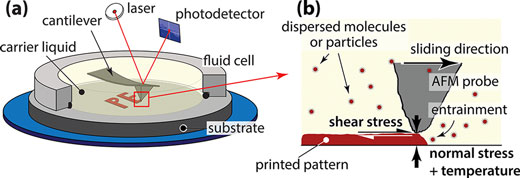 |
| Fig. 1: (a) Schematic of the NTP process on a substrate, using an AFM microcantilever submerged in an ink-containing fluid carrier in the fluid cell. (b) Schematic illustration of the entrainment of dispersed ink units at the leading edge of the sliding AFM probe, resulting in the stress-assisted formation of robust surface-bound solid structures on the substrate. (Reprinted with permission by American Chemical Society) |
| The choice of liquid carrier is determined primarily by the solubility and dispersion stability of ink units. During sliding, the molecules or nanoparticles in the ink are entrained into the contact at the leading edge of the AFM probe, as illustrated in Figure 1b above. |
| Once within the contact, applied normal and shear stresses result in surface-mediated tribochemical or tribomechanical interactions between multiple ink units, as well as ink units and the substrate, leading to the formation of stable surface-bound solidified structures. |
| "There are two aspects of this research that are quite exciting," Khare points out: "One, we are able to generate structures at the nanoscale additively, using only applied pressure and, sometimes, some heat. This is unusual in its relative simplicity to other additive nanolithography methods that require special working environments or operation conditions." |
| "Secondly" he adds, "the structures we are able to create exhibit remarkable mechanical properties. We report on measured moduli and hardness of structures created through NTP that approach values normally seen in bulk materials." |
| This technique has the potential to enable additive nanomanufacturing of mechanically robust structures, which in addition to certain thermal, electronic or optical functionality, are uniquely able to also withstand applied normal and shear stresses. |
| Practical applications of this technique could be in the fields of nanophotonics, sensors and wear-resistant nanoscale coatings. |
| The team is currently investigating other potential material systems, which could be used for ink materials in this technique. They are also pursuing methods to optimize and improve rates of patterning to increase throughput. |
| "One of the key challenges for this method, which also motivates the future direction of our research is scalability and throughput," Carpick concludes. "Given the serial nature of patterning in an AFM, patterning of large areas is intrinsically time-consuming and slow. We are currently investigating novel methods to improve patterning throughput using Nanotribological Printing." |
 By
Michael
Berger
– Michael is author of four books by the Royal Society of Chemistry:
Nano-Society: Pushing the Boundaries of Technology (2009),
Nanotechnology: The Future is Tiny (2016),
Nanoengineering: The Skills and Tools Making Technology Invisible (2019), and
Waste not! How Nanotechnologies Can Increase Efficiencies Throughout Society (2025)
Copyright ©
Nanowerk LLC
By
Michael
Berger
– Michael is author of four books by the Royal Society of Chemistry:
Nano-Society: Pushing the Boundaries of Technology (2009),
Nanotechnology: The Future is Tiny (2016),
Nanoengineering: The Skills and Tools Making Technology Invisible (2019), and
Waste not! How Nanotechnologies Can Increase Efficiencies Throughout Society (2025)
Copyright ©
Nanowerk LLC
|

Become a Spotlight guest author! Join our large and growing group of guest contributors. Have you just published a scientific paper or have other exciting developments to share with the nanotechnology community? Here is how to publish on nanowerk.com. |
