| Posted: Apr 08, 2008 |
Producing isolated nanocrystalline diamond fibers at high growth rates |
| (Nanowerk Spotlight) Diamonds have been known in India for at least 3000 years and are thought to have been first recognized and mined there. The most familiar usage of diamonds today is as gemstones in jewelry but, apart from being a girl's best friend, it seems that diamonds, especially nanodiamonds, are quickly becoming a scientist's best friend as well. Diamonds are the hardest natural material - the word diamond comes from the Greek term adamas, which means 'invincible' - has the lowest coefficient of thermal conductivity, is electrically insulating, chemically inert, and optically transparent. In nanoparticulate form, diamonds possess an additional property that makes them so interesting for researchers: since they are carbon-based and non-toxic they are a suitable material for drug delivery, drug diagnostics and medical imaging applications. |
| Recently, diamond-coated metallic and nonmetallic nanocomposite materials have gained a lot of attention in the scientific community. These nanocomposite structures have a better stiffness/weight ratio than any other existing material and thus have many potential applications in various strategic fields such as biosensors, energy applications, thermal management, and space technology. |
| Diamond is also a very good candidate for solid-state electronic emitters because of its negative or very low electron affinity. Electron emitters can be used in vacuum microelectronics such as Spindt-type emitters. There are many reports concerning field emission from chemical vapor deposited diamond or diamond-like carbon thin films. Up to now, however, only a few examples on synthesis and field emission studies from tubular nanorods or nanowhiskers diamond-based systems have been published. These diamond-based nanoscale structures have been prepared by common – but very expensive – methods, either e-beam lithography or reactive ion etching. |
| One of the challenges in fabricating nanodiamond coatings and composite materials is the difficulty of controlling the size, texture, and crystalline quality of the diamond particles. Now, researchers in Portugal have demonstrated for the first time the facile fabrication and the conformal coating of nanocrystalline diamond onto silica nanofibers by a two-step method: synthesis of templates on silicon wafer; and coating of the silica fibers with nanocrystalline diamond. |
| "We prepared, for the first time, high-density nanocrystalline diamond (NCD) fibers with lengths of 50–100 µm and diameters of 1–5 µm using amorphous silicon dioxide (a-SiO2) nanofiber templates" Dr. Manoj Kumar Singh tells Nanowerk. "The templates were synthesized by a conventional Vapor-Liquid-Solid (VLS) growth process followed by conformal coating of as-synthesized templates with 15–20 nm-sized NCD grains using a high-power microwave plasma enhanced chemical vapor deposition technique (MPECVD). We confirmed not only the nanocrystalline nature of the diamond material but also the perfect crystallinity of the sample." |
| Singh, a principal investigator in the TEMA-NRD Nanotechnology Research Division in the Department of Mechanical Engineering at the University of Aveiro in Portugal, explains that, unlike other reports on NCD fibers, this novel method can produce isolated nanocrystalline diamond fibers at high growth rates. |
| The researchers expect this novel material to find applications in cold-cathode devices, heat sinks in microelectronics and structural materials in micro- and nanoelectromechanical systems. |
| The scientists have reported their findings in the February 16, 2008 online edition of Chemistry of Materials ("Novel Two-Step Method for Synthesis of High-Density Nanocrystalline Diamond Fibers"). |
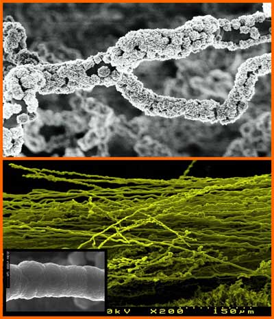 |
| The FE-SEM image shows the growth stages from nucleation to continuous fibrous structure formation of high-density diamond fibers. Insert shows high magnification image of a perfect NCD fiber. (Image: Dr. Singh, University of Aveiro) |
| Using their simple and low-cost technique, the NRD team synthesized high-density nanocrystalline diamond fibers with lengths of more than 500 µm. After synthesizing the silica nanofiber templates, the researchers treated the substrates with nanodiamond powder (particle size 3–5 nm) using the dip method, thereby randomly attaching nanodiamond particles on the surface of a-SiO2 nanofibers by capillary forces. The nanodiamond particles act as seeds for the further growth of NCD on the nanofibers. |
| Singh points out that the seeding process is a very critical phase for conformal coating as well as for controlling the diameter of NCD fibers. |
| The scientists also observed that during the MPECVD process the nanodiamond (particle size ∼15 nm) does not nucleate directly on the a-SiO2 surface but instead an intermediate layer of amorphous carbon is formed and the nanodiamond nucleates directly onto this layer during CVD growth. |
| Singh says that the team is now in the process of optimizing their technique. He adds: "We are also greatly interested in the development of NCD fiber reinforced polymer nanocomposites for biomedical applications and also as heat sinks in microelectronics." |
| In separate work, published in the January 18, 2008 online edition of Applied Physics Letters, the scientists reported the fabrication of patterned nanocrystalline diamond submicrometer-tip arrays with length of ∼10 µm and diameters of 1–2 µm, using the same method ("Electron field emission from patterned nanocrystalline diamond coated a-SiO2 micrometer-tip arrays"). |
 By
Michael
Berger
– Michael is author of four books by the Royal Society of Chemistry:
Nano-Society: Pushing the Boundaries of Technology (2009),
Nanotechnology: The Future is Tiny (2016),
Nanoengineering: The Skills and Tools Making Technology Invisible (2019), and
Waste not! How Nanotechnologies Can Increase Efficiencies Throughout Society (2025)
Copyright ©
Nanowerk LLC
By
Michael
Berger
– Michael is author of four books by the Royal Society of Chemistry:
Nano-Society: Pushing the Boundaries of Technology (2009),
Nanotechnology: The Future is Tiny (2016),
Nanoengineering: The Skills and Tools Making Technology Invisible (2019), and
Waste not! How Nanotechnologies Can Increase Efficiencies Throughout Society (2025)
Copyright ©
Nanowerk LLC
|

Become a Spotlight guest author! Join our large and growing group of guest contributors. Have you just published a scientific paper or have other exciting developments to share with the nanotechnology community? Here is how to publish on nanowerk.com.
