| Posted: May 25, 2006 |
A new fabrication method for nanospring technology |
| (Nanowerk Spotlight) Nanosprings, which are helical nanowires grown via a modified vapor-liquid-solid (VLS) mechanism, are of interest to researchers because of their potential applications in biological and chemical sensors, high porosity applications such as fuel cells, and biomedical drug delivery applications. Thanks to a novel fabrication method, nanosprings can now be synthesized with a yield higher than 90%, and with 100% repeatability. |
| Nanosprings come in a variety of flavors including boron carbide, silicon carbide and silicon dioxide. Nanosprings can be formed from any material as long as nanowires of that material can grow by VLS. So far, it was not possible to synthesize large quantities of nanosprings with uniform properties and through a repeatable process. In addition, the incompatibility of the majority of the synthesis processes with current semiconductor integrated circuit technologies poses another hurdle for the large scale application of nanosprings. |
| VLS growth occurs when a catalyst droplet resting on a surface absorbs wire-building material from a surrounding vapor. Once the concentration of the building material reaches super-saturation in the droplet, a portion of the material is secreted out the droplet base, and a wire gradually forms. Under some circumstances, the material deposition is asymmetrical and the wire develops into a helical nanospring. |
| In all cases of helical growth, such as carbon nanotubes or nanosprings, a mechanism must exist that introduces an asymmetry to the growth. In the case of nanosprings formed from a single amorphous nanowire, it is the existence of contact angle anisotropy at the interface between the nanowire and the catalyst that introduces the asymmetry. |
| However, for nanosprings formed from multiple wires, this mechanism does not apply. At this time there is no definitive explanation as to why multiple nanowires form from a single catalyst and it has been proposed that the mechanism behind the asymmetry is a competition between the nanowires forming the multi-nanowire nanosprings. |
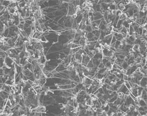 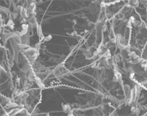 |
| SEM images of silica nanosprings (Source: Prof. David N. McIlroy, University of Idaho) |
| The University of Idaho maintains a research project dedicated to nanosprings and they recently achieved significant progress in nanospring synthesis, opening the door to their wider use. The W. M. Keck Nanosprings Project focuses on the controlled growth of nanosprings, measurement of their mechanical properties, and the development of nanospring devices. Professor David N. McIlroy, who leads the project, explains his recent findings to Nanowerk: |
| "The significance of our recent work is the development of a process that is repeatable and can be controlled at a level that facilitates integration into existing technologies or fabrication processes." The findings were reported in a paper titled "High yield synthesis and lithography of silica-based nanospring mats" published in the May 19, 2006 online edition of Nanotechnology. |
| There are three aspects to this work that make it amenable to technology development. |
| "First" says McIlroy, "is that the processing temperature for the nanosprings is as low as 350° C, or lower. This low processing temperature means that nanosprings can be deposited onto the surface of any material that can withstand this temperature in oxygen. Consequently, our nanospring process is compatible with flexible substrates." |
| "In addition, this process is compatible with silicon based VLSI technology" McIlroy points out. "Next is the ability to control the location of nanosprings using lithographic patterning." |
| Consequently, this process can be integrated into existing devices that are constructed using lithography and complex patterning of the nanospring mat can be achieved. |
| The final important breakthrough is the immense surface area of the nanosprings relative to a linear nanowire. For example, one nanospring can form from multiple nanowires and because of the coiling have orders of magnitude more surface area per unit length relative to a linear nanowire. |
 By
Michael
Berger
– Michael is author of four books by the Royal Society of Chemistry:
Nano-Society: Pushing the Boundaries of Technology (2009),
Nanotechnology: The Future is Tiny (2016),
Nanoengineering: The Skills and Tools Making Technology Invisible (2019), and
Waste not! How Nanotechnologies Can Increase Efficiencies Throughout Society (2025)
Copyright ©
Nanowerk LLC
By
Michael
Berger
– Michael is author of four books by the Royal Society of Chemistry:
Nano-Society: Pushing the Boundaries of Technology (2009),
Nanotechnology: The Future is Tiny (2016),
Nanoengineering: The Skills and Tools Making Technology Invisible (2019), and
Waste not! How Nanotechnologies Can Increase Efficiencies Throughout Society (2025)
Copyright ©
Nanowerk LLC
|

Become a Spotlight guest author! Join our large and growing group of guest contributors. Have you just published a scientific paper or have other exciting developments to share with the nanotechnology community? Here is how to publish on nanowerk.com.
