| Feb 21, 2020 |
Experimental identification of the foremost AFM tip atom |
| (Nanowerk Spotlight) The foremost atom of the tip in a scanning probe microscope is critically important for precise imaging results – similar to role of the objective lens in an optical microscope. In atomic force microscopy, the front atom significantly affects atomic-scale contrast and atom manipulation. |
| "The chemical species is a dominant factor in determining the tip state, and in situ chemical identification of a tip apex remains a challenging task," Dr. Jo Onoda from the Department of Physics at the University of Alberta, tells Nanowerk. "In spite of the successes in the chemical identification and electronegativity determination of surface atoms with Pauling’s equation, the possibility of chemically identifying tip apex atoms by this method has not been explored." |
| Electronegativity, an important theoretical concept in chemistry, was originally defined by Linus Pauling as ‘the power of an atom in a molecule to attract electrons to itself’ (JACS, "The nature of the chemical bond. IV. The energy of single bonds and the relative electronegativity of atoms"). |
| Pauling suggested that the bond energies of heterogeneous polar covalent bonds is expressed by the geometric mean of the homogeneous bond energies of the constituent atoms. This has been true for ensemble systems such as gaseous phase but has not been obvious for atomic-scale systems with a small number of atoms. |
| In a previous study (Physical Review Letters, "Chemical and Crystallographic Characterization of the Tip Apex in Scanning Probe Microscopy"), researchers attached CO molecules on a metal surface at very low temperature (4 K) and obtained AFM images that reflect the tip's own crystal structures; the method is like a 'selfie'. |
| By contrast, the new method relies on the measurement of chemical bond energy between tip and pre-characterized atoms and can be used even at room temperature. |
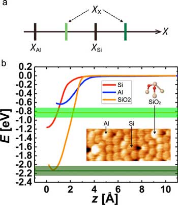 |
| Electronegativity determination of surface atoms solely by experiments. (a) Magnitude relationships of electronegativities for Si,Al, and unknown X atoms. (b) Short-range E(z) curves obtained on Si (red), Al (blue) adatoms, and SiO2 (orange), respectively. The expected values of bond energy on SiO2 acquired by the Al tip are represented by light and dark green lines with their error bands. The inset shows a typical topographic AFM image of Si, Al adatoms, and SiO2 on the Si(111)-(7x7) surface. The ball-and-stick model of SiO2 represents Si in cream and O in red. (Reprinted with permission by American Chemical Society) |
| In new work, published in Nano Letters ("Chemical Identification of the Foremost Tip Atom in Atomic Force Microscopy"), Onoda and his coauthors found that Pauling's equation is applicable to the analysis of tip apex atoms. The team also demonstrated a way to determine electronegativity of surface atoms solely by experiments. |
| "Thus, we can expect not only the direct application of our method to other systems but also new methodologies to analyze experimental results based on the Pauling's equation," Onoda points out. |
| "While the trend in the AFM community for the past decade has been the high-resolution imaging by physical interactions (such as Pauli repulsive forces) with CO-functionalized tips, we have been pursuing the potential of chemical bond forces and energies," Onoda notes. "Our research has been progressing from the chemical identification of surface atoms ("Chemical identification of individual surface atoms by atomic force microscopy"); the electronegativity determination of surface atoms; and then finally the present work: the chemical identification of a tip apex atom." |
| The scientists say that they still do not fully understand the theoretical background of their method and why the geometric mean of the Pauling's equation is the best descriptive model. To explore these issues they need to develop further theoretical verifications. |
| According to the team, they also need to obtain more information of the scatter plots of bond energies for various elements. The accumulation of the knowledge would make it easier to identify the chemical identities of unknown atoms. |
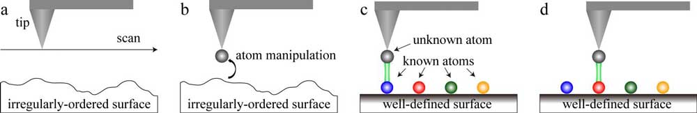 |
| A procedure for identifying the chemical element of an unknown atom sampled from the irregularly-ordered surface of an actual material. a) The surface of an actual material is imaged by AFM. b) The AFM tip is moved to the area to be analyzed and then used to pick up an atom that we would like to chemically identify. c) The AFM tip with the unidentified atom at its apex is brought to well-defined surfaces (such as Si(111) - (7×7)) on which chemically-identified elements are deposited. d) The energy spectroscopy is carried out on the identified atoms on the well-defined surface, and finally the identity of the tip apex atom is identified using our method. (Reprinted with permission by American Chemical Society) (click on image to enlarge) |
| From a practical viewpoint, this requires the preparation of a number of different tip states to complete the scatter plot of bond energies. The preparation of a large number of tips could require some automation in future work. |
| Since this method also opens a purely experimental way to determine the electronegativity of surface atoms, a promising application area could be the development of functional materials for instance for catalysis. |
| "One potential direction for our field is the AFM observation of emerging 2D materials such as silicene, germanene, and multi-component 2D alloys," Onoda concludes. "While AFM imaging with CO-functionalized tips shows clear surface structures for planar molecules and surfaces, it gives us complicated features for the buckled surface such as silicene. Reactive tips are useful for high-resolution imaging of such systems and our method is basically applicable to them." |
 By
Michael
Berger
– Michael is author of four books by the Royal Society of Chemistry:
Nano-Society: Pushing the Boundaries of Technology (2009),
Nanotechnology: The Future is Tiny (2016),
Nanoengineering: The Skills and Tools Making Technology Invisible (2019), and
Waste not! How Nanotechnologies Can Increase Efficiencies Throughout Society (2025)
Copyright ©
Nanowerk LLC
By
Michael
Berger
– Michael is author of four books by the Royal Society of Chemistry:
Nano-Society: Pushing the Boundaries of Technology (2009),
Nanotechnology: The Future is Tiny (2016),
Nanoengineering: The Skills and Tools Making Technology Invisible (2019), and
Waste not! How Nanotechnologies Can Increase Efficiencies Throughout Society (2025)
Copyright ©
Nanowerk LLC
|

Become a Spotlight guest author! Join our large and growing group of guest contributors. Have you just published a scientific paper or have other exciting developments to share with the nanotechnology community? Here is how to publish on nanowerk.com. |
