| Sep 10, 2020 |
Bottom-up fabrication of nanoelectronics with DNA nanotechnology |
| (Nanowerk Spotlight) At first glance, electronics and DNA, the fundamental building block of our genetic makeup, appear to be two completely different things. As it turns out, DNA could be particularly useful for the design of nanoscale electric circuits because it self-assembles, it self-replicates and it can adopt various states and conformations (read more about the ongoing development of DNA nanotechnology and why it has become such an intense nanotechnology research field). |
| In short, DNA is probably the most programmable biomaterial for creating a wide range of rationally designed and functionally enhanced nanostructures. |
| The fragile nature of pure DNA molecules and their non-established charge transport (different DNA transport experiments have shown that DNA may be insulating, semiconducting, or metallic) makes it unlikely that DNA could be employed directly as electronic materials. It could, however, be used as a template material for the fabrication of nanoelectronics. |
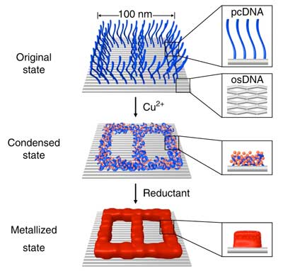 |
| Illustration of condensation and subsequent site-specific metal plating processes for fabricating a digit 8 pattern on a single-origami breadboard with a size of 100 × 70 nm2. (reprinted from Nat. Commun. 2019, 10 (1), 5597) |
| The term nanoelectronics refers to the use of nanotechnology in electronic components. These components are often only a few nanometers in size. However, the tinier electronic components become, the harder they are to manufacture. |
| That is why there is so much research interest in DNA nanotechnology for nanoelectronics – sophisticated, programmable, and addressable DNA nanostructures are strong candidates for constructing nanoelectronic devices. The size of DNA molecules is also key: DNA double-helix has a neighboring base pair distance of 0.34 nm, a hydrated diameter of 2.6 nm and a dehydrated diameter of 2.1 nm, and thus DNA complex-based nanoelectronics may break the 5-nm processing limit of commercial silicon-based semiconductors. |
| A recent review article in Nano Letters ("DNA-based fabrication for nanoelectronics") introduces the history of DNA-based fabrication for nanoelectronics briefly, and summarizes the state-of-the-art advances of DNA-based nanoelectronics. |
| Conductive metal, polymers and semi-conductive materials are important components in nanoelectronics. Challenges to achieve superior performance include accurate manipulation of the components and scaling down the size for higher integration level. Bottom-up assembly of DNA-based hybrid materials enables control with near-atomic-scale precision. Moreover, it reduces the instrumental cost compared with traditional lithographic methods, such as dip-pen and electron-beam lithography (EBL). |
| In their section 'DNA-templated Assembly of Electronic Materials', the authors introduce how inorganic metal, organic polymers and carbon nanotubes incorporate into well-ordered DNA nanostructures as well as their electronic properties. |
| Following that, the authors describe and discuss the most widely applied characterization techniques to explore DNA complex-based electronics' unique electronic properties, including scanning tunneling microscopy (STM), conductive atomic force microscopy (cAFM) and Kelvin probe force microscopy (KPFM). |
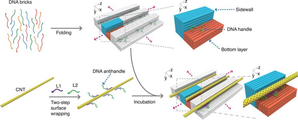 |
| Scheme of DNA hybridization-mediated CNT alignment based on DNA nanotrenches. The blue and the orange bundles represent the sidewall and the bottom layer, respectively, within a feature-repeating unit of trench-like DNA templates. Pink arrows indicate the extension directions of the repeating units. (Reprinted from Science 2020, 368 (6493), 874-877) (click on image to enlarge) |
| The closing section lists remaining challenges and open questions: |
| 1) It is worth noting that large-scale synthesis and practical application of DNA-based electronic materials generally lack, which is directly related to the scaling-up of DNA nanostructures, either assembling size or total yields. Scaling-up of two-dimensional DNA arrays assembly is a breakthrough, which will facilitate the connections between DNA based devices to electrodes. |
| 2) Metallized DNA nanostructures have not been applied in nanoelectronics due to the limited precision and lack of detailed metallization mechanism. This may lead to low yields and difficulties in precise conjugation. Meanwhile, granular structures or the existence of nonspecific nanoparticle deposition will impede the electronic behaviors. Productivity and reproducibility of metallic structures with well-defined size, shape, and morphology may be improved by theoretical calculations and discovery of new metallization systems. |
| 3) Although conductive polymer chain templated by DNA origami can form into 3D conformation, it is difficult to fabricate three-dimensional structures with required electronic properties. |
| 4) The accuracy limit of DNA nanotechnology has not been fully explored in electronics, as it has been proved that Bohr radius resolution of molecular placing can be realized using DNA origami. Is the 0.34 nm base pair distance limitation approachable for post assembled materials on DNA structures? Note that semiconducting silicon is not the only choice here, thus quantum tunneling induced efficacy-losing during dimension-shrinking can potentially be solved by carbon-based materials such as carbon nanotubes. |
| 5) Controlled multi-heterogenous materials assembly is still lacking, which is essential for building electronic devices. Although pioneered works have shown that quantum dots, metal nanoparticles can be packed together, in-depth understandings of local environments surrounding DNA nanostructures in various reaction processes are needed. |
 By
Michael
Berger
– Michael is author of four books by the Royal Society of Chemistry:
Nano-Society: Pushing the Boundaries of Technology (2009),
Nanotechnology: The Future is Tiny (2016),
Nanoengineering: The Skills and Tools Making Technology Invisible (2019), and
Waste not! How Nanotechnologies Can Increase Efficiencies Throughout Society (2025)
Copyright ©
Nanowerk LLC
By
Michael
Berger
– Michael is author of four books by the Royal Society of Chemistry:
Nano-Society: Pushing the Boundaries of Technology (2009),
Nanotechnology: The Future is Tiny (2016),
Nanoengineering: The Skills and Tools Making Technology Invisible (2019), and
Waste not! How Nanotechnologies Can Increase Efficiencies Throughout Society (2025)
Copyright ©
Nanowerk LLC
|

Become a Spotlight guest author! Join our large and growing group of guest contributors. Have you just published a scientific paper or have other exciting developments to share with the nanotechnology community? Here is how to publish on nanowerk.com. |
