| Posted: May 12, 2008 |
High resolution surface potential imaging with ultrasharp carbon nanotubes |
| (Nanowerk Spotlight) With the advance of nanotechnologies the demand for ever more precise instruments that measure, map and manipulate details at the nanoscale increases as well. For instance, the study of potential distributions with nanoscale resolution becomes increasingly important. In the early days of atomic force microscopy (AFM) the scanning force microscope was used to measure charges, dielectric constants, film thickness of insulating layers, photovoltage, and electrical potential of a given surface. Then, in 1991, the concept of a scanning contact potential microscope was introduced, allowing the simultaneous measurement of topography and contact potential difference. Named the scanning surface potential microscope (SSPM) – also often referred to as Kelvin probe force microscope – this is a variation of the AFM that measures the electrostatic forces (potential) between the probe tip and the surface of a material. |
| The conducting tip and the sample are characterized by (in general) different work functions – i.e. the minimum energy needed to remove an electron from a solid to a point immediately outside the solid surface (the work function is an important property of metals). SSPM is conducted by a two pass technique. During the first pass line scan, the sample topography is imaged by normal tapping mode. The second pass raises the probe above the sample by a fixed distance (10 nm here) and measures the surface potential, following the previous-recorded topography to maintain a constant tip-sample distance. |
| Compared with other AFM techniques, the lateral resolution of traditional SSPM, from submicron down to 10 nm, is much lower. Furthermore, the SSPM-measured potential does not truly represent the local surface potential because all three parts of an AFM probe (tip apex, tip cone, and cantilever itself) can contribute to the long-range electrostatic forces that are central to SSPM operation. |
| Researchers have now solved this problem by mounting ultra sharp and high aspect ratio carbon nanotube (CNT) bundles onto the apex of an AFM tip, which effectively reduces the non-local electrostatic interactions. This technique markedly improves the SSPM technique in its spatial and potential resolution, making it a better tool for surface potential mapping at the nanoscale. |
| "Our findings provide direct experimental observations that ultra high aspect ratio AFM probes can enhance the potential contrast up to several factors for sub micron features" Dr. Minhua Zhao explains to Nanowerk. "That is to say, the underestimation of potential measurement using a standard AFM probe can be very severe. In the meantime, the ultra sharpness at the end of CNT bundles also improves the lateral resolution (<2 nm) of our SSPM measurement, the best results achieved at ambient condition so far." |
| Zhao, now a researcher at NIST/NIH, first-authored a recent paper about this work in Nanotechnology ("Ultrasharp and high aspect ratio carbon nanotube atomic force microscopy probes for enhanced surface potential imaging") while a postdoc in Prof. Bryan Huey's group at the University of Connecticut's Institute of Materials Science (IMS). |
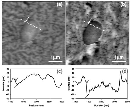 |
| Surface potential mapping of purple bacteriorhodopsin (BR) membrane fragments with total gray scale contrast of 120 mV via (a) conventional AFM probes and (b) high aspect ratio CNT AFM probes. (c) Potential profile along the segmented line by a conventional AFM probe; the potential change is ∼8 mV between the two arrows in a distance of 47 nm. (d) Potential profile along the segmented line by a CNT AFM probe. The potential change is ∼32 mV between the two arrows in a distance of 47 nm. (Reprinted with permission from IOP Publishing) |
| The IMS team's motivation to conduct this work was that commercially available probes did not meet their needs. Zhao says that the aspect ratio of silicon AFM probes is not high enough, while CNT length of a commercial CNT AFM probe is too short to sufficiently reduce the non-local electrostatic interactions. |
| "The ultrasharpness at the end of CNT bundles is the key to high lateral resolution SSPM imaging" Zhao points out. "The enhanced and high resolution surface potential imaging that we achieved by ultrasharp and high aspect ratio CNT AFM probes is especially critical for nanoscale features of low potential contrast, with promising applications in the semiconductor industry and biotechnology such as dopant mapping, and label-free protein detection." |
| The CNT AFM probes were prepared using an AC dielectrophoresis technique (for more details see: "Control of Length and Spatial Functionality of Single-Wall Carbon Nanotube AFM Nanoprobes") where single-walled CNTs were first purified and shortened and then 'sharpened' to approximately 10 nm near the apex by gold/palladium sputtering (in fact, the entire probe is coated with AU/Pd to remove the distortion at the end of the bundle). |
| Zhao explains that, when a standard AFM probe is used, the SSPM-measured potential depends on the feature size – which is a problem when trying to identify a material based on its potential difference. In contrast, when an ultra high aspect ratio probe is used for potential measurement, it is much less sensitive to the feature size, making it possible to identify a material based on its surface potential. |
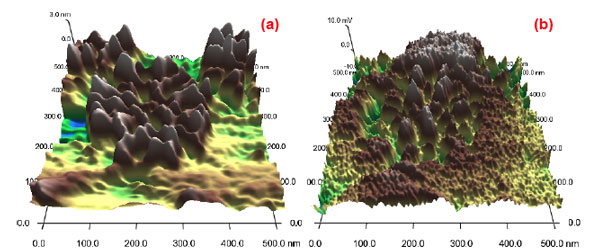 |
| High resolution AFM imaging of self-assembled BRs on HOPG substrate by an ultra sharp and high aspect ratio CNT AFM probe. Image size is 500 nm. (a) 3D topography image. (b) 3D surface potential imaging. The protruding features in topography correspond to sinking ones in potential. (Reprinted with permission from IOP Publishing) |
| Another unique feature of the prepared CNT AFM probes is their ultra-sharpness at the end of CNT bundles. "Under certain conditions, there is only one SWCNT with diameter smaller than 1 nm protruding from the CNT bundles" says Zhao. "Hence, high spatial resolution SSPM images are also possible by these probes." |
| The potential applications for this work is very broad, such as dopant mapping and failure analysis of integrated circuit chip in semiconductor industry, label-free biomolecules detection for medical research, and nanoscale chemical imaging of materials based on SSPM-measured potential. |
 By
Michael
Berger
– Michael is author of four books by the Royal Society of Chemistry:
Nano-Society: Pushing the Boundaries of Technology (2009),
Nanotechnology: The Future is Tiny (2016),
Nanoengineering: The Skills and Tools Making Technology Invisible (2019), and
Waste not! How Nanotechnologies Can Increase Efficiencies Throughout Society (2025)
Copyright ©
Nanowerk LLC
By
Michael
Berger
– Michael is author of four books by the Royal Society of Chemistry:
Nano-Society: Pushing the Boundaries of Technology (2009),
Nanotechnology: The Future is Tiny (2016),
Nanoengineering: The Skills and Tools Making Technology Invisible (2019), and
Waste not! How Nanotechnologies Can Increase Efficiencies Throughout Society (2025)
Copyright ©
Nanowerk LLC
|

Become a Spotlight guest author! Join our large and growing group of guest contributors. Have you just published a scientific paper or have other exciting developments to share with the nanotechnology community? Here is how to publish on nanowerk.com.
