| Posted: Jun 03, 2008 |
One molecule thick nanotechnology membranes take shape |
| (Nanowerk Spotlight) Since its discovery in 2004, graphene has created quite a buzz among scientists (Nanotechnology researchers go ballistic over graphene). The reason they are so excited is that two-dimensional crystals (it's called 2D because it extends in only two dimensions - length and width; as the material is only one atom thick, the third dimension, height, is considered to be zero) open up a whole new class of materials with novel electronic, optical and mechanical properties. For instance, the ultimate size limit for a nano-electromechanical system (NEMS) would be a nanoscale resonator that is only one atom thick, but this puts severe constraints on the material; as a single layer of atoms, it should be robust, stiff, and stable. Graphene, the simplest of the 2D conjugated carbon nanomaterials, could fit that bill. |
| One hurdle for researchers is that current methods for the synthesis of two-dimensional, carbon-rich networks have many limitations including lack of molecular-level control and poor diversity. In a step to overcome these obstacles, researchers have now developed new synthetic strategies for forming monolayer films of conjugated carbon, in various configurations ranging from flat 2D sheets, to balloons, tubes and pleated sheets. |
| "We have shown that linked carbon monolayers can be formed on a variety of solid surfaces" John A. Rogers tells Nanowerk. "These linked monolayers are synthesized by linking three different alkyne-containing monomers with two different carbon–carbon bond-forming reactions. The linked monolayers synthesized on flat surfaces have extremely large aspect ratios and are easily transferred from the native surface by protecting with photoresist and etching the inorganic substrate." |
| These monolayer membranes developed by Rogers, a professor of chemistry, materials science and engineering at the University of Illinois at Urbana-Champaign, together with his organic chemist collaborators in Dr. Jeff Moore's group are sufficiently robust to be suspended over 440-nm diameter holes without tearing. |
| The linked monolayers were also prepared on structured surfaces and 3D supports, and the freestanding monolayer membranes maintained the shape of the original support after etching. |
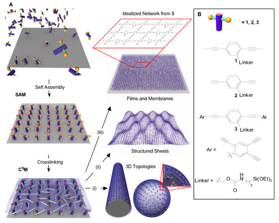 |
| Schematic illustration of linked monolayer formation. Self-assembled monolayers (SAMs) are synthesized on a substrate, then cross-linked to form linked monolayers. This approach is applied to the formation of 3D topologies (i), structured sheets (ii), and membranes (iii). The box above iii provides an idealized view of the chemical structure for a linked monomer network formed from monomer 3. (Reprinted with permission from PNAS) |
| "Our approach to the synthesis of monolayer carbon networks provides a powerful method to explore the properties and device applications of a wide variety of carbon films" says Rogers. "We are currently exploring other linking chemistries and monomers for the synthesis of conducting, 2D monolayer films." |
| The process developed by the University of Illinois researchers involves two steps: (1) solution phase formation of a self-assembled monolayer of molecules on a substrate, via covalent bonding between one of the ends of the molecules to the surface, and (2) chemical crosslinking reactions that establish covalent bonds between adjacent molecules in this monolayer. |
| This two-step process creates crosslinking, 2D films of carbon, whose chemistry is defined by the choice of the precursor molecules (which are separately synthesized, and can therefore incorporate nearly arbitrary choices of functional groups). This process can be carried out on flat substrates (e.g. silicon wafers) or curved (cylinders, spheres) or structured surfaces. |
| Rogers explains that transfer printing methods allow these materials to be moved and manipulated for device integration and fundamental studies. "Our work yields a new class of material that might be interesting for various applications in nanotechnology, ranging from porous molecular filter membranes to transport layers in field effect transistors" he says. |
| These nanomembranes are related to, but different from, graphene sheets. In particular, they do not have the structural perfection of graphene, but they allow much more scalable synthesis and ability to incorporate chemically diverse structures. |
| "Our materials have the potential to offer excellent mechanical, thermal and electrical properties in a type of material that, due to its mode of synthesis, would be immediately suitable for large scale device integration" Rogers points out. "This capability is absent, for example, from widely studied small pieces of graphene formed by mechanical exfoliation from bulk pieces of graphite." |
| There is quite a number of potential applications for this material. One is molecular-scale separation membranes for chemical or biochemical analysis. Because their method gives them a high degree of control over the composition of the membranes, their structure could be fine-tuned to make them useful as molecular sieves. |
| Other possibilities include electronics, where this material might be useful as an alternative to the more widely explored polymer and small molecule organic semiconductors, for flexible electronics, displays and related devices. In further improved versions, Rogers hopes to achieve high performance, suitable for applications in areas such as RF electronics. |
| In its current form, the carbon monolayers are not suitable yet for applications in high-performance electronics. The scientists say that a main challenge is to create long range, crystalline like order in these systems to improve the electrical properties. "One strategy that we are pursuing involves the use of crystalline substrates for the formation of the monolayers in the first step of the process," says Rogers. |
| One of Roger's research foci is on printable and flexible electronics (Gutenberg + nanotechnology = printable electronics) and he believes that the carbon monolayers would be suitable for creating films for flexible displays to be used in handheld devices or computer screens. |
| The University of Illinois team describes their findings in a paper published online on May 27, 2008 in PNAS ("Synthesis of linked carbon monolayers: Films, balloons, tubes, and pleated sheets"). |
 By
Michael
Berger
– Michael is author of four books by the Royal Society of Chemistry:
Nano-Society: Pushing the Boundaries of Technology (2009),
Nanotechnology: The Future is Tiny (2016),
Nanoengineering: The Skills and Tools Making Technology Invisible (2019), and
Waste not! How Nanotechnologies Can Increase Efficiencies Throughout Society (2025)
Copyright ©
Nanowerk LLC
By
Michael
Berger
– Michael is author of four books by the Royal Society of Chemistry:
Nano-Society: Pushing the Boundaries of Technology (2009),
Nanotechnology: The Future is Tiny (2016),
Nanoengineering: The Skills and Tools Making Technology Invisible (2019), and
Waste not! How Nanotechnologies Can Increase Efficiencies Throughout Society (2025)
Copyright ©
Nanowerk LLC
|

Become a Spotlight guest author! Join our large and growing group of guest contributors. Have you just published a scientific paper or have other exciting developments to share with the nanotechnology community? Here is how to publish on nanowerk.com.
