| Posted: Jun 12, 2008 |
Converting plastic into light-emitting nanostructures |
| (Nanowerk Spotlight) Light-emitting nanostructures are widely used for optical, photonic, chemical, and biological devices. For example, fluorescent nanoparticles are useful for biological assays and as tumor markers, chemical sensors, and organic lasers, whereas one-dimensional luminescent nanowires are exploited for novel nanoscale photonic devices such as nano-lasers and nanowire scanning microscopy. While several methods to prepare organic, inorganic, and polymeric light-emitting nanostructures have been developed, the fabrication of luminescent nanoarchitectures with a tailored morphology and pattern is still challenging. |
| Luminescent nano- and microparticles are generally fabricated by incorporating fluorescent materials, such as dyes and quantum dots, into non-emissive particles. Conventional methods to produce luminescent nanopatterns require two or more individual steps: synthesizing luminescent materials and fabricating the nanopatterns. Researchers in Korea have discovered that non-luminescent polystyrene can be converted into a luminescent organic material whose emitting color can be tuned from deep blue to white by electron irradiation. They demonstrated that luminescent nanopatterns are readily fabricated only by irradiating an electron beam to the selected regions of polystyrene. In addition, the top-down irradiation approach in conjunction with self-assembled polystyrene nanostructures allows fabrication of diverse and complex luminescent nanoarchitectures. |
| "We have presented a strategy to obtain luminescent nanoarchitectures based on a simple one-step electron irradiation process" Dr. Sung Oh Cho tells Nanowerk. "Electron irradiation produces light- emitting materials from non-luminescent polymers while simultaneously patterning the polymer to form nanostructures. Our top-down irradiation strategy, through combination with bottom-up approaches for precursor preparation or through direct electron-beam writing, provides a powerful tool to fabricate desired complex luminescent nanoarchitectures and nanopatterns." |
| The strategy developed by Cho, an Associate Professor in the Department of Nuclear and Quantum Engineering at the Korea Advanced Institute of Science and Technology (KAIST), and his team utilizes solution-processable polymeric material as a precursor and the polymer surface can be easily functionalized to respond to chemical, biological, electronic, and optical stimuli. |
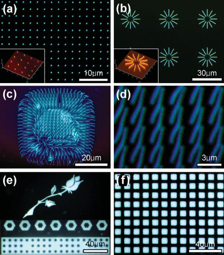 |
| Patterned light-emitting nanostructures and microstructures. Fluorescence microscopy images of a) luminescent nanodots (diameter: ∼100 nm) and b) nanowires (lateral width: ∼100 nm) arrays. The insets are AFM topography images of the nanodot and nanowire arrays, respectively. c) Assembly of luminescent nanowires. The lateral width of the nanowires is 200nm and the length of the nanowires is 12 µm. d) Array of luminescent nanowires aligned on a silicon substrate. The nanowires have a lateral width of 200nm and a length of 5 µm, respectively. e) Fluorescence microscopy images of light-emitting microstructures with diverse morphologies such as a rose, hexagonal microrings, and circular micropores. f) Light emissive pixel arrays patterned using a 2000-mesh copper grid as a mask. (Reprinted with permission from Wiley-VCH Verlag) |
| The KIST scientists believe that the approach presented here will be useful for a wide range of research fields including optics, photonics, chemistry, and biology. |
| They describe their findings in a paper published online on May 5, 2008 in Advanced Materials ("Fabrication of Luminescent Nanoarchitectures by Electron Irradiation of Polystyrene"). |
| "As is well known, diamond is an electrical insulator, whereas graphite is a good conductor although both are carbon allotropes" Cho describes the background to their work. "We thought that if we synthesize carbon materials that have a chemical structure between diamond and graphite, the carbon material can have semiconducting properties. Many previous studies including ours already showed that irradiation of an electron beam or an ion beam onto organic polymers could induce hydrogenated amorphous carbon which has a mixed structure of diamond-like sp3 carbon and graphite-like sp2 carbon. Thus, we thought that electron-irradiated polymer could have semiconducting properties." |
| Based on this idea, Cho and his collaborators tried to irradiate electron beam onto many organic polymers and investigated whether the irradiated polymers emit visible light, because common semiconductors emit visible light with the wavelength corresponding to the bandgap under the excitation. |
| "We found that most of the electron-irradiated organic polymers emitted visible light when excited with ultraviolet light; especially polystyrene showed most strong emission light" he says. "We found that aromatic rings inside polystyrene were aggregated to form polycyclic aromatic hydrocarbons (PAHs) by electron irradiation. Because of the cyclic conjugated structure of the aromatic rings, PAHs show interesting luminescent properties. The average number of the clustered aromatic rings of the generated PAHs increased with increasing the electron irradiation time, which explains why the emitting color of the irradiated polystyrene can be changed by changing the electron dose." |
| This technique also allows fabrication of desired light emission patterns by irradiating selective regions of polystyrene films with an electron beam. |
| The KAIST team observed that electron-irradiated polystyrene is superior to commercial light-emitting polymers (LEPs) in its stability against photo- and thermal-oxidation. Many LEPs, or conjugated polymers, have already been commercialized. However, most of the commercialized LEPs have a drawback of easy oxidation and thus the lifetime of a device fabricated with the LEPs is relatively short. |
| The Korean team's preliminary study showed that irradiated polystyrene – possibly due to PAHs – has a much higher thermal- and photo-oxidative stability than commercialized LEPs. This superior emission stability makes the new technique very attractive in producing devices with long-life characteristics. |
| Cho points out that the team found that the electrical conductivity of the irradiated polystyrene is not so good compared to commercially available conjugated polymer. "We will further develop our irradiation technique: by changing the polymer precursor and by controlling the irradiation parameters, we will try to synthesize organic materials that have both good electrical and good optical properties" he says. "Then, using the electron-irradiated polymers, we will fabricate organic electronic and optical devices such as organic solar cells, organic thin film transistors, and organic light emitting diodes." |
 By
Michael
Berger
– Michael is author of four books by the Royal Society of Chemistry:
Nano-Society: Pushing the Boundaries of Technology (2009),
Nanotechnology: The Future is Tiny (2016),
Nanoengineering: The Skills and Tools Making Technology Invisible (2019), and
Waste not! How Nanotechnologies Can Increase Efficiencies Throughout Society (2025)
Copyright ©
Nanowerk LLC
By
Michael
Berger
– Michael is author of four books by the Royal Society of Chemistry:
Nano-Society: Pushing the Boundaries of Technology (2009),
Nanotechnology: The Future is Tiny (2016),
Nanoengineering: The Skills and Tools Making Technology Invisible (2019), and
Waste not! How Nanotechnologies Can Increase Efficiencies Throughout Society (2025)
Copyright ©
Nanowerk LLC
|

Become a Spotlight guest author! Join our large and growing group of guest contributors. Have you just published a scientific paper or have other exciting developments to share with the nanotechnology community? Here is how to publish on nanowerk.com.
