| Apr 28, 2022 |
Perovskite photovoltaics for a greener Internet-of-Things |
| (Nanowerk Spotlight) Perovskites are a family of crystals that show promising properties for applications in nanotechnology, especially nanostructured solar cells. Perovskite is a term used to describe a group of materials that have a distinctive crystal structure of cuboid and diamond shapes. They have long been of interest for their superconducting, electronic and ferroelectric properties (read more in our primer on Perovskites). |
| A perovskite solar cell is a type of solar cell, which includes a perovskite structured compound, most commonly a hybrid organic-inorganic lead or tin halide-based material, as the light-harvesting active layer. |
| Perovskite materials are usually cheap to produce and relatively simple to manufacture. Perovskites possess intrinsic properties like broad absorption spectrum, fast charge separation, long transport distance of electrons and holes, long carrier separation lifetime, and more, that make them very promising materials for solid-state solar cells. |
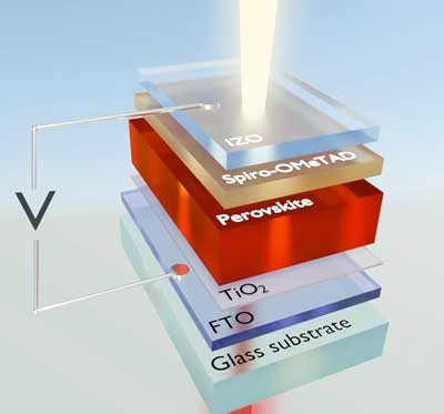 |
| Perovskite solar cells convert a high fraction of incident light directly into usable current. (Image: Fabian Ruf/Scilight) |
| Perovskite solar cells are causing excitement within the solar power industry with their ability to absorb light across almost all visible wavelengths, exceptional power conversion efficiencies, and relative ease of fabrication. |
| Put simply, perovskite solar cells aim to increase the efficiency and lower the cost of solar energy. |
| The amount of power required for many indoor electronics and small personal wireless electronics ranges from microwatts to hundreds of milliwatt. Implantable and other bioelectronic systems such as hearing aids and cochlear implants require even less and range from nanowatt to tens of milliwatt. |
| This power level can be supplied by organic and perovskite photovoltaics upon harvesting the photon energy in indoor settings and converting it to electrical energy, providing power densities in the range of several tens of microwatt per square centimeter, as recently demonstrated. |
 |
| Key requirements for organic and perovskite photovoltaic technologies to become the next generation power sources for microelectronic applications. (Reprinted with permission by Wiley-VCH Verlag) |
| The Internet-of-Things (IoT) is a huge worldwide network of connected objects. These 'things' are embedded with sensors, processors and software to collect and share data about the way they are used and about the environment around them. An Internet of Things platform integrates data from the different devices and applies analytics to share the most valuable information with applications built to address specific needs. |
| Most IoT devices are deployed inside buildings, so indoor photovoltaics could serve as a key technology for powering these. According to predictions, the number of IoT connected devices will grow dramatically to 75 billion in 2025 and a staggering 125 billion by 2030. At that point, there will be almost 15 things connected to the Internet for each human on earth. |
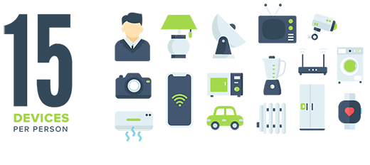 |
| It is estimated that by 2030, for each human on earth there will be almost 15 things connected to the Internet. (Source: reply.com) |
| A recent progress report compares emerging indoor photovoltaic technologies with alternative energy harvesters (piezoelectric, triboelectric, thermoelectric, and ambient RF) and provides a great overview of this field ("Emerging Indoor Photovoltaic Technologies for Sustainable Internet of Things"). |
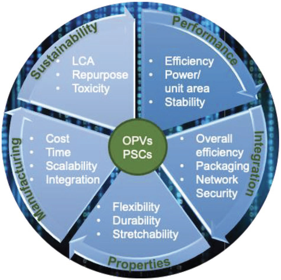
| As another recent review explains and addresses in great detail (Advanced Functional Materials, "Advances in Organic and Perovskite Photovoltaics Enabling a Greener Internet of Things"), the requirements that solar cells should satisfy to power IoT devices are quite different to the ones usually deemed necessary for application in outdoor-placed solar panels. |
| The size of the single solar cell used in IoT applications is much smaller, and in combination with the lower power input available in low-light indoor settings as well as the emission spectra of light sources other than the sun, renders the need for high conversion efficiency paramount. |
| Depending on the kind of IoT device, further requirements for photovoltaics ,for instance in bioelectronic and wearable systems, are light weight and flexible mechanical properties such as bendability and stretchability. |
| Increasingly important in an era of heightened ecological concerns is the use of abundant non-toxic and biodegradable materials, accompanied by green fabrication protocols and methods, and recyclability and/or reusability at the end of life. |
| For the flexible electronics industry this specifically means: 1) reduction of electronic waste (e-waste); 2) lowering the power consumption of electronic devices; and 3) elimination or reduction of toxic materials and hazardous substances used in electronics manufacturing. |
| Specifically with regard to IoT applications, the two photovoltaic technologies, which share similar processing and device fabrication protocols – organic and perovskite photovoltaic technologies – could be integrated in tandem structures that merge their advantages. For instance, a low bandgap photoactive organic layer can harvest the near-infrared part of the spectrum, while the ambipolar high mobility perovskite layer ensures retaining of a high open-circuit voltage and efficiency. |
| One area where researchers across research areas and disciplines still have their work cut out for them is the requirement to achieve greener electronics. More specifically, the presence of toxic elements, particularly lead (Pb), in perovskite materials has been a matter of rigorous investigation within the research community. |
| One potential solution is the robust encapsulation of the photovoltaics to avoid environmental pollution during the device???s lifetime. However, that still leaves the requirement to retrieve and recycle the Pb from electronic devices at their end of life. |
| Organic semiconducting materials employed in organic photovoltaics and as transporting layers in perovskite solar cells at first glance appear more benign, as they do not contain toxic elements. Nevertheless, certain plastics, despite containing non-toxic elements, are known to cause health problems (some conjugated organic molecules and polycyclic aromatic hydrocarbons can be carcinogenic), while the solvents used during their chemical synthesis or film formation from their solution can be toxic to humans and/or aquatic life, thus representing an occupational and environmental hazard. |
| Researchers are working on replacing these solvents with aqueous or alcoholic ones. The key challenge here is to alter the material and/or the solvent and yet succeed in controlling the film morphology that defines photovoltaic properties. |
 By
Michael
Berger
– Michael is author of four books by the Royal Society of Chemistry:
Nano-Society: Pushing the Boundaries of Technology (2009),
Nanotechnology: The Future is Tiny (2016),
Nanoengineering: The Skills and Tools Making Technology Invisible (2019), and
Waste not! How Nanotechnologies Can Increase Efficiencies Throughout Society (2025)
Copyright ©
Nanowerk LLC
By
Michael
Berger
– Michael is author of four books by the Royal Society of Chemistry:
Nano-Society: Pushing the Boundaries of Technology (2009),
Nanotechnology: The Future is Tiny (2016),
Nanoengineering: The Skills and Tools Making Technology Invisible (2019), and
Waste not! How Nanotechnologies Can Increase Efficiencies Throughout Society (2025)
Copyright ©
Nanowerk LLC
|

Become a Spotlight guest author! Join our large and growing group of guest contributors. Have you just published a scientific paper or have other exciting developments to share with the nanotechnology community? Here is how to publish on nanowerk.com. |
