| Posted: Jun 17, 2008 |
Nanolens makes color imaging of nano objects possible |
| (Nanowerk Spotlight) Optical imaging of materials is full with rich physical, chemical and biological information about the sample, because the optical energies in the visible range coincide with the atomic and molecular transition energies of many materials. Apart from the topographical information, the optical image therefore contains information about intrinsic properties of a material. However, the wave nature of light prevents the light to focus in a volume smaller than half of the wavelength, which is about 200-300 nm for visible light. Therefore, it is almost impossible to image nanomaterials, which could be a few nanometers in size, using optical imaging process. A typical lens made of, for example glass, will not be sufficient to image a nanomaterial. |
| In work that gives rise to a new concept of a lens for optical imaging, scientists in Japan have proposed a lens made of silver nanorods, rather than a curved glass surface. This metallic nanolens is capable of manipulating light in such a way that an optical image of nanoscale objects can be obtained in the visible range. |
| "We have demonstrated that our nanolens can transfer color images of nanoscale objects over distances of at least micrometer scale with a sufficient amount of magnification for far-field observation" Dr. Prabhat Verma tells Nanowerk. "We believe that, in principle, the image can be transferred over even longer distances without any significant loss. The proposed nanolens could potentially be a strong imaging tool, for example, for observing individual viruses and other nano-entities in the far field." |
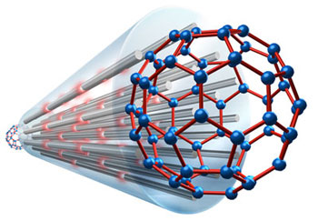 |
| Optical energy transfers plasmonically through the lengths of silver nanorods. Illustration of long-distance image transfer through a metallic nanolens that provides a magnified colour image with subwavelength spatial resolution (Image: Dr. Verma) |
| Verma, an Associate Professor in the Nano-Biophotonics Group in the Department of Frontier Biosciences at Osaka University, Japan, together with collaborators from the Department of Applied Physics at Osaka University and the Nanophotonics Laboratory at RIKEN, has published these findings in the June 15, 2008 online edition of Nature Photonics ("Subwavelength colour imaging with a metallic nanolens"). |
| A metal always has free change carriers – called plasmons – moving collectively on the surface of the metal. Plasmons play a large role in the optical properties of metals since they can interact with light, and somehow manipulate the predicted nature of light. |
| "Inspired by this possibility, some researchers proposed sub-wavelength imaging of nano-objects through metal" explains Verma. "However, there were several practical problems with this. One of the most important restriction was that only one particular wavelength that resonates with the plasmons can be used in imaging, which essentially means that a normal colored object – which emits many wavelengths – would not make a sharp image. The other problem was that the plasmons lose energy quite quickly as they propagate, making it impossible to have a long distance image transfer. Last, but not the least, the size of the image remained the same as the object (in the nanometer scale), and thus it was impossible to record these images." |
| The researchers in Japan overcame all these problems with the design of a nanolens that involves a tapered stacked arrangement of silver nanorods. The layers are separated by nano-gaps, which prevents the propagation of plasmons, resulting in extremely low loss of energy and thus making long distance imaging possible. It appears that a gap size of 10 nm gives the optimum value for efficient imaging. |
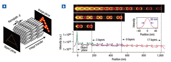 |
| Long-distance image transfer can be realized through a stacked arrangement of nanorod arrays. a, The basic concept of the stacked arrangement of nanorod arrays for long-distance image transfer. In this example, a three-layered stacked arrangement is presented. The image of the letter ?A? is obtained from simulations based on three-dimensional finite-difference time-domain (3D-FDTD) calculations. b, Intensity profiles across 3-, 9-, and 17-layered stacked arrays, showing that neither intensity nor the point spread function has any noticeable dependence on distance, at least up to micrometer-scale distances. The inset shows the line width of the point spread function at the exit of 17 layers. (Reprinted with permission from Nature Publishing Group) |
| Color imaging requires the resonance to be broad, so that a large part of the visible spectrum can be covered. "Our simulation results show that with an increasing number of layers, the number of resonant modes also increases, and they tend to gather in the vicinity of the fundamental mode of the corresponding unit rod" Verma describes the results. "Moreover, the nanolens can also magnify the image so that the image can be large enough for normal viewing." |
| This technique has the potential to be an indispensable imaging tool, in particular, for bio-medical applications, where individual viruses and other nano-objects of different colors could be simultaneously imaged at a long distance and could be detected at sufficient magnification with usual microscopes and detectors, such as a CCD camera. |
| The proposed silver nanolens is a conceptual visualization supported by rigorous calculations and simulations. Verma points out that the obvious next step is a practical fabrication of the proposed device. |
| "A potential challenges lies in the accurate growth of silver nanorods with precise geometry, which involves growth of stacked arrays of silver nanorods where the arrays are separated with specific nano-gaps and are arranged in a tapered manner" he says. "We are optimistic that the present rapid advances in growth techniques will make this possible in the very near future." |
 By
Michael
Berger
– Michael is author of four books by the Royal Society of Chemistry:
Nano-Society: Pushing the Boundaries of Technology (2009),
Nanotechnology: The Future is Tiny (2016),
Nanoengineering: The Skills and Tools Making Technology Invisible (2019), and
Waste not! How Nanotechnologies Can Increase Efficiencies Throughout Society (2025)
Copyright ©
Nanowerk LLC
By
Michael
Berger
– Michael is author of four books by the Royal Society of Chemistry:
Nano-Society: Pushing the Boundaries of Technology (2009),
Nanotechnology: The Future is Tiny (2016),
Nanoengineering: The Skills and Tools Making Technology Invisible (2019), and
Waste not! How Nanotechnologies Can Increase Efficiencies Throughout Society (2025)
Copyright ©
Nanowerk LLC
|

Become a Spotlight guest author! Join our large and growing group of guest contributors. Have you just published a scientific paper or have other exciting developments to share with the nanotechnology community? Here is how to publish on nanowerk.com.
