| Posted: Jul 05, 2006 |
A novel method for mass production of nanotube based electronics |
| (Nanowerk Spotlight) The mass production of nanoelectronic devices has been hampered by difficulties in aligning and integrating the millions of nanotubes required for the job. Now, researchers in South Korea have developed a method to precisely assemble and align single-walled carbon nanotubes (SWCNTs) onto solid substrates without relying on external forces such as electric or magnetic fields. This result could be an important guideline for the large-scale directed-assembly of integrated devices based on SWCNTs. |
| Professor Seunghun Hong from the Hybrid Nano-Device & Nano-Assembly Lab at Seoul National University explained the findings to Nanowerk: |
| "Even though various devices based on carbon nanotubes or nanowires showed capabilities superior to conventional silicon-based devices, a lack of mass-production methods for such devices has been holding back their practical applications. Since most nanotubes and nanowires are first synthesized in solution or powder forms, one has to pick up and assemble individual nanotubes/nanowires onto solid substrates to build functional devices, which can be an extremely time-consuming task." |
| Hong and his colleagues recently reported their findings in a paper titled "Directed-assembly of single-walled carbon nanotubes using self-assembled monolayer patterns comprising conjugated molecular wires" published in the June 26, 2006 online edition of Nanotechnology. Therein they describe their newly developed method to precisely assemble and align SWCNTs onto solid substrates without relying on external forces. |
| "In our method, SWCNTs are selectively adsorbed onto polar self-assembled monolayer (SAM) patterns comprised of conjugated molecular wires in the solution, while non-polar SAM is utilized to avoid non-specific adsorption of SWCNTs" Hong says. "Importantly, we found that by utilizing non-polar SAM as passivation layer, we can induce the "self-alignment" of SWCNTs along desired directions without relying on external forces. Furthermore, SAM of conjugated molecular wires works as a conducting layer providing good electrical contacts between SWCNTs and electrodes." |
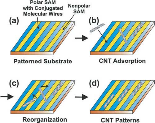 |
| Schematic diagram depicting the directed-assembly of carbon nanotubes using SAM patterns comprising conjugated molecular wires. (Reprinted with permission from IOP Publishing Ltd.) |
| Previous works about directed-assembly relied mostly on molecular wires with alkane backbones which are known to be relatively poor conductors. SAM with alkane backbones may result in poor contact resistance between SWCNTs and electrodes. Herein, we achieved large-scale directed assembly of SWCNTs utilizing SAM patterns comprising conjugated molecular wires such as 2MI, 2MP and 4MP. They have π-conjugated backbones and are believed to be highly conducting molecular wires. |
| Hong is confident that they can apply their method for the mass production of nanowire/nanotube-based electronic devices such as nano-size transistors, logic circuits, chemical sensors, bio sensors, etc. "Eventually" he says, "we are pursuing complete integration of nanowire/nanotube-based devices with conventional silicon electronics for ‘hybrid device architecture’." |
 By
Michael
Berger
– Michael is author of four books by the Royal Society of Chemistry:
Nano-Society: Pushing the Boundaries of Technology (2009),
Nanotechnology: The Future is Tiny (2016),
Nanoengineering: The Skills and Tools Making Technology Invisible (2019), and
Waste not! How Nanotechnologies Can Increase Efficiencies Throughout Society (2025)
Copyright ©
Nanowerk LLC
By
Michael
Berger
– Michael is author of four books by the Royal Society of Chemistry:
Nano-Society: Pushing the Boundaries of Technology (2009),
Nanotechnology: The Future is Tiny (2016),
Nanoengineering: The Skills and Tools Making Technology Invisible (2019), and
Waste not! How Nanotechnologies Can Increase Efficiencies Throughout Society (2025)
Copyright ©
Nanowerk LLC
|

Become a Spotlight guest author! Join our large and growing group of guest contributors. Have you just published a scientific paper or have other exciting developments to share with the nanotechnology community? Here is how to publish on nanowerk.com.
