| Mar 22, 2023 |
Shaping with light - a novel method for crafting chiral nanostructures with lasers |
| (Nanowerk Spotlight) Chirality is a property of objects that exist in different forms that are mirror images of each other but cannot be superimposed, like left hand and right hand. It is a common phenomenon in the universe and has many practical applications, especially in creating special materials called chiral nanostructures. |
| Chiral nanostructures, characterized by their unique mirror-image formations, possess special qualities that make them useful for information storage and light detection in advanced electronic devices designed to manipulate and detect specific types of light. |
| However, creating artificial chiral nanostructures, particularly with semiconductor materials, is challenging. Most current methods for making them, especially for semiconductors, are often complex and lack the necessary control and versatility. |
| Researchers at Wuhan University in China have now demonstrated a new way to create chiral nanostructures using a laser beam. By carefully controlling the direction of the laser beam's vibrations, the researchers created a variety of chiral structures made of platinum oxide in unique shapes, like twisted micropillars and spiral superstructures. This method also works for other semiconductors, like cadmium sulfide. |
| "Our new approach offers many possibilities for creating advanced materials, which could be used in devices like sensors and optical systems that can manipulate and detect chiral light," Prof. Tao Ding, who leads the Photonic Materials and Technology group in the School of Physics and Technology at Wuhan University, tells Nanowerk. |
| The team reported their findings in PNAS ("Optical dipole-induced anisotropic growth of semiconductors: A facile strategy toward chiral and complex nanostructures"). |
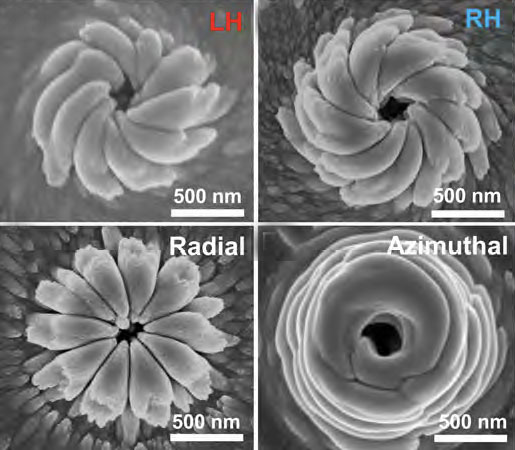 |
| Fabrication of spiral nanostructures with vector beams. SEM images of platinum oxide nanostructures generated by irradiating the precursor solution with different types of vector beams. (Image adapted from doi:10.1073/pnas.2216627120) |
| "In our work we show a new method for creating chiral semiconductor structures at the nanoscale using laser light without needing any additional particles," explains Ding. "These chiral nanostructures have interesting properties that make them useful for controlling and manipulating special types of light. Our simple and versatile approach could lead to the development of advanced materials for devices like advanced sensors and optical systems that can work with chiral light. We are also contemplating to use it for chiral photocatalysis and chiral molecule sensing." |
| The team's work shows that it is possible to grow anisotropic nanoparticles using photochemical deposition (Anisotropic means having different properties in different directions. In this context, this is because they are grown in a specific way that causes them to have a specific shape). This process involves the interaction between light and certain chemicals to grow the particles. The growth of these particles is influenced by the direction of the light's vibrations, creating a difference in how they grow compared to other directions. |
| This is a significant finding because it creates a new paradigm for the fabrication of chiral nanostructures and could lead to the development of new types of advanced sensors or solar cells. Additionally, these nanoparticles could be used to create new types of optical displays. |
| "What is exciting about this is that it is the first demonstration that materials can be stacked and twisted with the rotation of polarization, which show tunable chiroptic property," Ding points out. "It has never been so easy to do this with nanoscale materials and now you can stack and twist them like Lego blocks." |
| Building on their results, the researchers are now exploring additional functionality of this material system, such as its optoelectronic responses, as well exploring more materials that can be fabricated in the same way and the generation of enhanced chiral light emission. |
|
"Scalable fabrication is another aspect we want to address as we progress and begin to shape this into a patent application," Ding concludes.
|
 By
Michael
Berger
– Michael is author of four books by the Royal Society of Chemistry:
Nano-Society: Pushing the Boundaries of Technology (2009),
Nanotechnology: The Future is Tiny (2016),
Nanoengineering: The Skills and Tools Making Technology Invisible (2019), and
Waste not! How Nanotechnologies Can Increase Efficiencies Throughout Society (2025)
Copyright ©
Nanowerk LLC
By
Michael
Berger
– Michael is author of four books by the Royal Society of Chemistry:
Nano-Society: Pushing the Boundaries of Technology (2009),
Nanotechnology: The Future is Tiny (2016),
Nanoengineering: The Skills and Tools Making Technology Invisible (2019), and
Waste not! How Nanotechnologies Can Increase Efficiencies Throughout Society (2025)
Copyright ©
Nanowerk LLC
|

Become a Spotlight guest author! Join our large and growing group of guest contributors. Have you just published a scientific paper or have other exciting developments to share with the nanotechnology community? Here is how to publish on nanowerk.com. |
