| Oct 10, 2023 |
Inkjet-printed touchscreens gain a third dimension |
| (Nanowerk Spotlight) Touch screens have become such a pervasive part of everyday life that it's easy to forget how revolutionary the technology once was. Since the first prototype touchscreens emerged in the 1960s, continual advances have driven the technology's evolution from novelty to ubiquity. Touchscreens now enable interactions with countless smartphones, tablets, computers and appliances worldwide. |
| But despite this progress, fundamental limitations remain with current touchscreen implementations. Most detect only the horizontal and vertical coordinates of touches, providing two-dimensional (2D) input. This restricts the types of touch gestures possible. Adding a third dimension—the ability to recognize touch pressure—would open up an array of new interface capabilities. Pressure sensitivity could enable more intuitive, expressive and functional touch interactions. |
| Researchers have now developed a novel method to create touch screens that can precisely detect the location and pressure of touches in 3D space. The technology, described in a paper published in Advanced Materials ("Three-Dimensional Touch Device with Two Terminals"), uses standard inkjet printing techniques to deposit electronic materials onto thin plastic films. This allows for simplified large-scale manufacturing compared to existing transparent touch screens. |
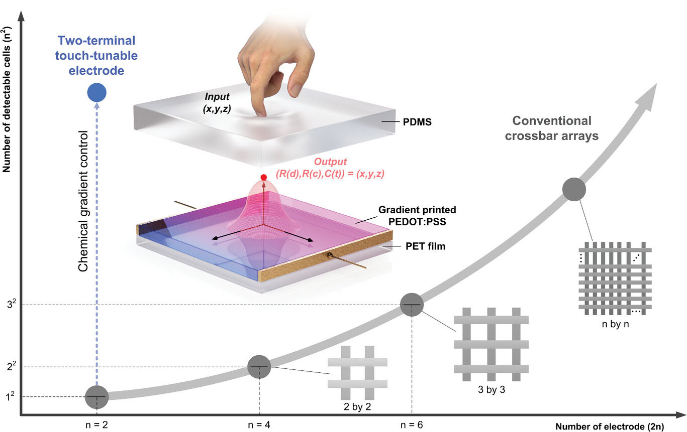 |
| Relationship between the number of detectable cells and the number of electrodes. The use of a two-terminal touch-tunable electrode facilitates the detection of a large number of cells without the need for a large number of electrodes. The inset shows a schematic of a 3D touch device with two terminals. The device comprises a polydimethylsiloxane (PDMS) layer and a chemically graded electrode poly(3,4-ethylenedioxythiophene) polystyrene sulfonate (PEDOT: PSS) layer on a substrate. (Reprinted with permission by Wiley-VCH Verlag) |
| "By providing a third dimension for input, entirely new kinds of touch gestures become possible," said Dr. Wooyoung Shim, materials scientist at Yonsei University in Seoul, South Korea and leader of the research team. "It allows touch screens to measure the force and trajectory of touches, which can enable advanced interface techniques and new applications." |
| The core of the technology is the use of transparent conductive films made from an organic polymer called PEDOT:PSS. By carefully controlling the composition of the polymer layer, the researchers created a position-dependent resistance profile over the surface of the film. This allowed a single pair of electrodes connected to the edge of the film to detect the precise location of touches from the changes in resistance. |
| Adding a thin pressure-sensitive dielectric layer on top enabled the films to additionally sense touch pressure from subtle changes in capacitance. Together, the resistance and capacitance changes provided enough information to reconstruct the precise 3D position and pressure of touches. |
| Crucially, the films retain their transparency, allowing their integration with display technologies to create interactive interfaces. And because the films can be deposited over large areas via printing, the approach is highly scalable. |
| "The simplicity of the device structure and manufacturability are its biggest strengths," said Shim. "In contrast to other transparent touch sensors, our approach minimizes device wiring and structures, allowing truly large-area touch sensing films to be produced efficiently." |
| Shim envisions touch interfaces produced using this technique having sensor densities exceeding 10,000 pixels per square inch, higher than existing consumer touch screens. This would enable tracking intricate touch movements and gestures precisely. |
| To demonstrate, the researchers printed a 10 x 10 cm transparent touchpad divided into a grid of sensing spots. When touches were applied to different spots with varying pressure, the system reconstructed the precise 3D tracking of the touches over time. This included recognizing complex multi-touch gestures. |
| The printed touch films showed excellent durability too, maintaining their sensing capabilities even when folded completely over on themselves. And tests revealed they could undergo 1,000s of bending cycles with little performance degradation - exceeding the durability of other transparent touch sensing technologies. |
| According to Shim, the ability to be flexed and folded repeatedly without damage points to many new possibilities. "It opens the door to foldable or conformable touch interfaces integrated onto irregular surfaces," he said. |
| In addition to touch screens and pads, Shim said the technology has promise for creating transparent 'skins' that can be wrapped over objects to make their surfaces touch sensitive. This could enable interactive surfaces for in-car dashboards, appliances, toys and more. The films even have potential for biomedical uses like markers for imaging tissues during surgery. |
| "We demonstrated a 'smart' artificial mouth that uses the films to detect the detailed movement and pressures of a model tongue," explained Shim. "This could form the basis of low-cost kits to help detect and diagnose language and swallowing disorders." |
| While promising, challenges remain to improve the spatial resolution and multi-touch capabilities of the printed touch films before widespread commercialization. But the combination of simplicity, scalability, durability and cost-effectiveness make the printing-based approach a promising candidate to help enable the next generation of touch interfaces and interactive surfaces. |
 By
Michael
Berger
– Michael is author of four books by the Royal Society of Chemistry:
Nano-Society: Pushing the Boundaries of Technology (2009),
Nanotechnology: The Future is Tiny (2016),
Nanoengineering: The Skills and Tools Making Technology Invisible (2019), and
Waste not! How Nanotechnologies Can Increase Efficiencies Throughout Society (2025)
Copyright ©
Nanowerk LLC
By
Michael
Berger
– Michael is author of four books by the Royal Society of Chemistry:
Nano-Society: Pushing the Boundaries of Technology (2009),
Nanotechnology: The Future is Tiny (2016),
Nanoengineering: The Skills and Tools Making Technology Invisible (2019), and
Waste not! How Nanotechnologies Can Increase Efficiencies Throughout Society (2025)
Copyright ©
Nanowerk LLC
|

Become a Spotlight guest author! Join our large and growing group of guest contributors. Have you just published a scientific paper or have other exciting developments to share with the nanotechnology community? Here is how to publish on nanowerk.com. |
