| Posted: Jul 16, 2008 |
Directed self-assembly of ordered structures as a simple nanotechnology tool |
| (Nanowerk Spotlight) The use of spontaneous self-assembly as a lithography- and external field-free means to construct well-ordered, often intriguing structures has received much attention for its ease of organizing materials on the nanoscale into ordered structures and producing complex, large-scale structures with small feature sizes. These self-organized structures promise new opportunities for developing miniaturized optical, electronic, optoelectronic, and magnetic devices. |
| An extremely simple route to intriguing structures is the evaporation-induced self-assembly of polymers and nanoparticles from a droplet on a solid substrate. However, flow instabilities within the evaporating droplet often result in non-equilibrium and irregular dissipative structures, e.g., randomly organized convection patterns, stochastically distributed multi-rings, etc. Therefore, fully utilizing evaporation as a simple tool for creating well-ordered structures with numerous technological applications requires precise control over several factors, including evaporative flux, solution concentration, and the interfacial interaction between solute and substrate. |
| To this end, a group of scientists has developed a simple and straightforward method to create gradient concentric rings of multi-walled carbon nanotubes (MWCNTs) over large surface areas with controlled density by combining two consecutive self-assembly processes, namely, evaporation-induced self-assembly of polymers in a sphere-on-flat geometry, followed by subsequent directed self-assembly of MWCNTs on the polymer-templated surfaces. |
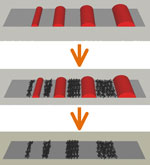 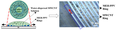 |
| Left: Schematic stepwise representation of formation of gradient concentric MWCNT rings. Evaporation-driven self-assembly of MEH-PPV rings on silicon substrate from MEH-PPV toluene solution in a sphere-on-flat geometry. Then a drop of MWCNT/PDDA water solution was drop-cast onto the MEH-PPV ring-patterned silicon substrate. Upon completion of water evaporation, MWCNT rings were formed in between MEH-PPV rings. After selective removal of MEH-PPV with toluene, gradient concentric MWCNT rings can be revealed. Center: Drop-cast the MWCNT solution over the entire surface of ring patterns. Right: Optical micrograph during the formation of MWCNT rings. The water meniscus retreated along the MEH-PPV ring surface (i.e., dewetting on hydrophobic MEH-PPV ring), as indicated by an arrow in a dashed box, thereby forming two MWCNT rings adjacent to each other. (Images: Dr. Lin, Iowa State University) |
| "When compared to lithographic methods that involve expensive equipment and maintenance costs, our method is fast and cost-effective, dispensing with the need for multistage lithography and externally applied fields." Dr. Zhiqun Lin tells Nanowerk. "For our process to work, we only need a drop of polymer solution and CNT solution, and two simple tools: a spherical lens and silicon substrate." |
| Lin, an Assistant Professor in the Materials Science and Engineering Department at Iowa State University, and his group have been working on the development of a simple, one-step evaporation-based method for fabricating nanostructured materials with or without hierarchical order in a precisely controllable manner, dispensing with the need for lithography techniques and external fields. |
| They have reported results from this work – specifically the production of self-organized gradient concentric ring patterns – previously, such as "Spontaneous Formation of Mesoscale Polymer Patterns in an Evaporating Bound Solution" in a 2007 paper in Advanced Materials and "Evaporation-Induced Self-Assembly of Nanoparticles from a Sphere-on-Flat Geometry" in Angewandte Chemie International. In the latter work, the scientists have achieved 630-nm wide CdSe/ZnS quantum dot rings. |
| Further reducing the size of structures formed via evaporation-induced self-assembly to the nanometer scale currently is a particular challenge. Lin mentions that this may be done by tailoring a number of parameters, including the curvature of the spherical lens, the use of pre-patterned substrate, etc. |
| In their most recent work, published in the July 9, 2008 online edition of Advanced Functional Materials ("Directed Self-Assembly of Gradient Concentric Carbon Nanotube Rings"), Lin's team extends their simple and straightforward technique to create gradient concentric rings of CNTs over very large surface areas by combining two consecutive self-assembly processes. By using vaporation-induced self-assembly of polymer in a confined geometry consisting of a sphere on a flat silicon substrate, hundreds of gradient concentric polymer rings with remarkable regularity were spontaneously formed on the silicon substrate. The researchers then exploited the concentric polymer rings on the silicon as a chemically patterned surface to guide the formation of MWCNT rings. The formed concentric rings had a unique gradient feature. |
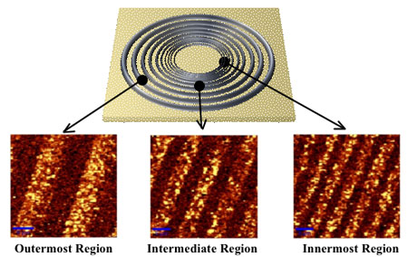 |
| Raman images of MWCNT rings on the silicon substrate. Left panel: at outermost region; middel panel: at intermediate region; and right panel: at innermost region. The scale bars are 6 µm, 5 µm, and 5 µm in left panel, middel panel, and right panel, respectively. The Raman intensity varied from dark (low) to bright (high) color. (Images: Dr. Lin, Iowa State University) |
| "The combination of spontaneous evaporation-induced self-assembly and subsequent directed self-assembly offers a new means of patterning microscopic CNT rings over large areas" explains Lin. |
| Lin adds that, by replacing MWCNTs with single-walled CNTs (SWCNTs), the formation of gradient concentric SWCNT rings from solution-based SWCNTs may be suitable for applications in electrics, optics, and sensors, for example, mass production of SWCNT-based electronic devices to explore the channel length effect on the mobility of SWCNTs in one step. |
| "Furthermore, our method can be extended to direct self-assembly of other nanomaterials such as nanoparticles, nanowires, and nanoribbons in a precisely controllable manner for use in photonics, electronics, optical materials, optoelectronics, nanotechnology, and biotechnology," he says. |
| The team have identified two issues that could further enhance their current method: using polymer templates of different shapes and improving the quality of the carbon nanotubes. Lin explains that the former can be achieved by guiding the controlled solvent evaporation using an upper surface of different shape (e.g., replacing the spherical lens with the square pyramidal lens to yield gradient concentric squares) in the restricted geometry. "For the latter, we can direct self-assembly of either exclusively metallic or exclusively semiconducting SWCNTs for use in electronics, optoelectronics, thin film transistors, and sensors." |
| The researchers' next step will be the attempt to create hierarchically ordered structures via the synergy of evaporation-driven self-assembly at the microscopic scale and spontaneous self-assembly at the nanoscopic scale. "Hierarchical structures with well-defined dimensions are formed by controlled solvent evaporation and associated capillary flow of the solute in restricted geometries," says Lin. "These structures may exhibit two or more independent characteristic dimensions, e.g., microscale concentric rings and self-organized nanoscopic constituents residing along these various dimensions." |
 By
Michael
Berger
– Michael is author of four books by the Royal Society of Chemistry:
Nano-Society: Pushing the Boundaries of Technology (2009),
Nanotechnology: The Future is Tiny (2016),
Nanoengineering: The Skills and Tools Making Technology Invisible (2019), and
Waste not! How Nanotechnologies Can Increase Efficiencies Throughout Society (2025)
Copyright ©
Nanowerk LLC
By
Michael
Berger
– Michael is author of four books by the Royal Society of Chemistry:
Nano-Society: Pushing the Boundaries of Technology (2009),
Nanotechnology: The Future is Tiny (2016),
Nanoengineering: The Skills and Tools Making Technology Invisible (2019), and
Waste not! How Nanotechnologies Can Increase Efficiencies Throughout Society (2025)
Copyright ©
Nanowerk LLC
|

Become a Spotlight guest author! Join our large and growing group of guest contributors. Have you just published a scientific paper or have other exciting developments to share with the nanotechnology community? Here is how to publish on nanowerk.com.
