| Jan 11, 2024 |
Precision growth technique for self-aligning organic nanowires |
| (Nanowerk Spotlight) The unique properties of organic semiconductors have driven their increasing use in advanced electronics and optoelectronics over the past decade. Compared to conventional inorganic materials, researchers can custom design the molecules to achieve specialized characteristics. Equally important is processability at low temperatures and easy integration with next-generation devices. However, a stubborn challenge has been the inability to control key growth parameters of nanoscale organic semiconductor structures that enable practical applications. |
| In particular, the paper utilizes a technique called graphoepitaxy – a mechanism where nanowires grow along the linear orientation defined by nanoscale surface features on a substrate, rather than the underlying crystalline structure. This graphoepitaxial guidance had already been used to align inorganic nanowires, but initial attempts to apply it for organic semiconductor structures like Alq3 yielded randomly scattered growths with no long-range order. |
| Now, an international team of researchers have reported an innovative extension of graphoepitaxy that enables simultaneous control over the alignment direction and location of organic semiconductor nanowires across a whole substrate during vapor deposition synthesis. |
| Published in Advanced Functional Materials ("Selective-Area Growth of Aligned Organic Semiconductor Nanowires and Their Device Integration"), the technique combines graphoepitaxial guidance from nanoscale surface features with microscale shadows from a mask to direct the growth of highly ordered organic nanowire arrays in predefined locations. |
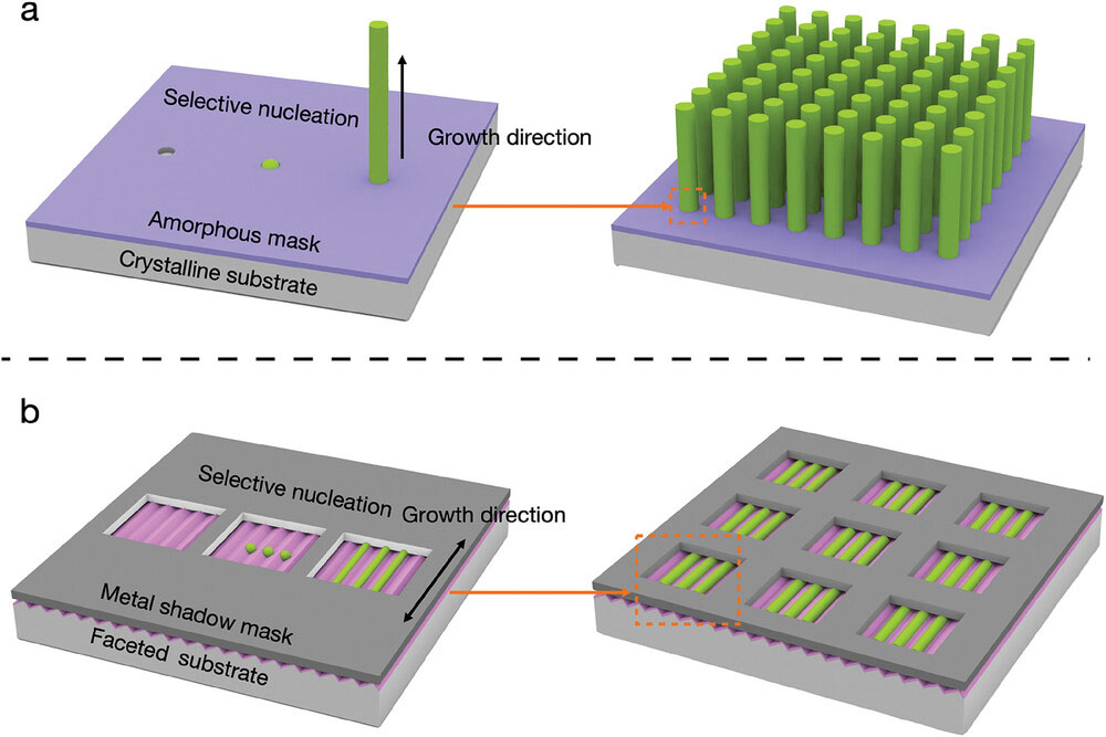 |
| Schematic diagrams of selective-area growth of nanowires in vapor phase. a) Previous selective-area out-of-plane epitaxial growth of aligned nanowires on a flat single-crystalline surface, where the nanowire positions are determined by nanoscale holes on the coated amorphous mask and the nanowire growth orientation is inherited from the underlying lattice-matched surface. b) Proposed selective-area in-plane graphoepitaxial growth of aligned nanowires on a faceted single-crystalline surface, where the nanowire positions are determined by micro-sized holes on the covered metal mask and the nanowire growth orientation is defined by the periodic facets of the surface. (Reprinted with permission by Wiley-VCH Verlag) |
| "Being able to dictate orientation and site-specificity of organic nanowires in a single growth process enables their seamless integration into functional devices without damaging manual manipulation,” explains lead author Dr. Jinyou Xu. |
| The new growth process utilized tris(8-hydroxyquinoline)aluminum (Alq3), an organic semiconductor and light emitter. Alq3 nanowires were synthesized using physical vapor deposition onto a tailored faceted sapphire surface that directed their orientation along parallel nanogrooves. This ‘graphoepitaxy’ mechanism had already guided inorganic nanowires but initial attempts with Alq3 produced randomly oriented ‘grassy’ growths with no long-range order. |
| Researchers found that modifying the faceted surface with an ultra-thin alkyl coating altered the surface energy balance and enhanced the interaction between Alq3 molecules during deposition. This promoted preferential horizontal alignment along the nanogrooves. But nanowire positions were still not controlled. |
| To localize growths to specific areas, researchers covered the surface with a shadow mask containing an array of microscale holes, restricting Alq3 vapor flux to only directly exposed regions. Computational fluid simulations revealed that holes induced non-uniform mass transport profiles and boundary layer thickness variations which confined the initial nanowire nucleation sites to small regions around hole centers. Owing to nanoscale geometry, these nucleation sites sent out unidirectional growth fronts that remained aligned to nanogrooves across entire holes. This combined ‘selective-area graphoepitaxy’ technique assembled arrays of highly oriented Alq3 nanowires with controlled densities and lengths based on hole layouts. |
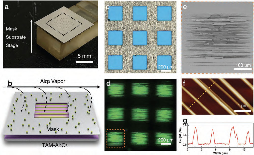 |
| Selective-area growth of self-oriented Alq3 nanowires. a) Digital photography and b) schematic diagram of the stacking configuration. The dashed square in (a) indicates the substrate position under the shadow mask. c) Optical microscopic image of the metal shadow mask. d) Fluorescence optical microscopic image of the site-controlled horizontally-aligned Alq3 nanowires under UV illumination. e) Representative SEM image of the sitecontrolled horizontally-aligned Alq3 nanowires in a micro-sized hole. f) AFM image and g) height profile of the Alq3 nanowires. (Reprinted with permission by Wiley-VCH Verlag) |
| Structural analyses using cross-polarized optical microscopy, electron diffraction and X-ray diffraction verified the single-crystalline nature of Alq3 nanowires with long-range molecular order and preferential growth axis along the (01̄1) lattice plane. An exceptional 75.12% internal quantum efficiency was measured. The aligning mechanism was not contingent on lattice-matching, unlike existing epitaxial growth techniques. Researchers demonstrated micro-scale control to generate oriented Alq3 nanowire arrays with different sizes and shapes across a substrate by simply adjusting hole parameters in the shadow mask. Notably, 872 micron long nanowires were obtained using rectangular holes – a length-to-diameter ratio exceeding 1200. |
| As-grown nanostructure arrays were directly integrated into functioning electronic devices without any nanowire transfer or manual manipulation. A two-terminal device exhibited strong negative differential resistance with a 3.97 peak-to-valley current ratio, competitive with state-of-the-art materials. This unusual conductivity profile is attractive for specialized circuit applications such as memories, amplifiers and logic switches. Additionally, a distinct photoresponse was measured under 405 nm illumination with 200 millisecond rise/decay times, confirming photosensitivity. |
| “The proposed selective-area graphoepitaxy method altered the long-held notion that lattice-matching between crystals is mandatory for controlling orientation. Furthermore, no metal catalysts were required,” explains Xu. “The technique opens possibilities of assembling various organic molecules into custom oriented nanowire architectures for electronics manufacturing.” |
| However, contact issues related to device fabrication need optimized electrode interfaces. Regardless, this breakthrough research makes a compelling case that synergistically harnessing self-assembly behaviors on multiple length scales enables scalable bottom-up nanomanufacturing not viable through top-down lithography. Importantly, it liberates organic nanowires from constraints of manual manipulation by directing site-specific orientation-controlled growths. |
 By
Michael
Berger
– Michael is author of four books by the Royal Society of Chemistry:
Nano-Society: Pushing the Boundaries of Technology (2009),
Nanotechnology: The Future is Tiny (2016),
Nanoengineering: The Skills and Tools Making Technology Invisible (2019), and
Waste not! How Nanotechnologies Can Increase Efficiencies Throughout Society (2025)
Copyright ©
Nanowerk LLC
By
Michael
Berger
– Michael is author of four books by the Royal Society of Chemistry:
Nano-Society: Pushing the Boundaries of Technology (2009),
Nanotechnology: The Future is Tiny (2016),
Nanoengineering: The Skills and Tools Making Technology Invisible (2019), and
Waste not! How Nanotechnologies Can Increase Efficiencies Throughout Society (2025)
Copyright ©
Nanowerk LLC
|

Become a Spotlight guest author! Join our large and growing group of guest contributors. Have you just published a scientific paper or have other exciting developments to share with the nanotechnology community? Here is how to publish on nanowerk.com. |
