| Posted: Jul 26, 2006 |
Connecting nanowires using nanoparticles |
| (Nanowerk Spotlight) One major challenge in much of nanotechnology is how to connect nanocomponents together. Despite significant advancements in nanowire growth techniques, establishment of electrical contacts to nanowire assemblies through non-destructive methods has not yet been successfully realized. Researchers now report a novel approach toward connecting and electrically contacting vertically aligned nanowire arrays using conductive nanoparticles. |
| "In our particular case we wanted to make electrical contacts to both ends of a nanowire array and still leave the array accessible to liquids or gases" says Professor Michael R. Zachariah, director of the Co-Laboratory for NanoParticle Based Manufacturing and Metrology at the University of Maryland and the National Institute of Standards and Technology (NIST). |
| Zachariah explained his lab's recent findings to Nanowerk: "We developed a new approach to electrically connect these wires using nanoparticles which would specifically attach to the ends of the wires. The particular application for which we wanted the electrical connection was for a gas sensor, however the method should be generic to any application where nanowire arrays require electric connectivity." |
| The research is described in a recent paper, titled "A universal approach to electrically connecting nanowire arrays using nanoparticles—application to a novel gas sensor architecture", published in the July 6, 2006 online edition of Nanotechnology. |
| The researchers devised and tested an original, generic approach toward achieving electrical contacts to vertically aligned ZnO nanowire arrays using electrostatically assisted deposition of gold nanoparticles. The Au nanoparticle electrode is observed to be both mechanically and electrically robust even at high temperatures. |
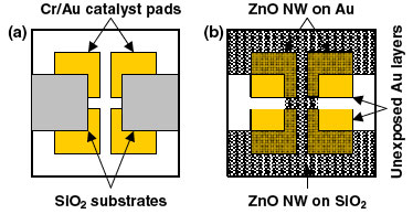 |
(a), (b) represent substrate surfaces before and after nanowire growth respectively. Clean SiO2 wafers were placed on top of the substrate before nanowire growth to enable electrical contact to the bottom of the nanowires grown on each individual catalyst pad. (Reprinted with permission from IOP Publishing) |
| The nanowires grown on the Au catalyst layer are well aligned along the vertical direction with widths between 60 and 80 nm, and lengths between 5 and 10 µm, while the nanowires on the adjacent SiO2 portion are more randomly oriented. |
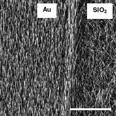 |
SEM image of ZnO nanowires grown on Au and SiO2 (left and right portions) clearly indicate alignment of nanowires on Au and lack of alignment on SiO2. Scale bar is 10 µm (Reprinted with permission from IOP Publishing) |
| Electrical contact to the top of the nanowire array was established by creating a contiguous nano-particle film through electrostatic attachment of conductive gold nanoparticles exclusively onto the tips of nanowires. |
| "This approach of creating a top contact to a vertically aligned nanowire assembly as grown, may be useful for the design and fabrication of electrically driven nanowire lasers and LEDs" says Zachariah. "Our first successful application of this nano-architecture is a gas sensing device, which exhibits high sensitivities to low concentrations (10 ppm to 50 ppm) of both reducing (methanol) and oxidizing (nitrous oxide) gases. |
| This assembly approach is amenable to any nanowire array for which a top contact electrode is needed. |
 By
Michael
Berger
– Michael is author of four books by the Royal Society of Chemistry:
Nano-Society: Pushing the Boundaries of Technology (2009),
Nanotechnology: The Future is Tiny (2016),
Nanoengineering: The Skills and Tools Making Technology Invisible (2019), and
Waste not! How Nanotechnologies Can Increase Efficiencies Throughout Society (2025)
Copyright ©
Nanowerk LLC
By
Michael
Berger
– Michael is author of four books by the Royal Society of Chemistry:
Nano-Society: Pushing the Boundaries of Technology (2009),
Nanotechnology: The Future is Tiny (2016),
Nanoengineering: The Skills and Tools Making Technology Invisible (2019), and
Waste not! How Nanotechnologies Can Increase Efficiencies Throughout Society (2025)
Copyright ©
Nanowerk LLC
|

Become a Spotlight guest author! Join our large and growing group of guest contributors. Have you just published a scientific paper or have other exciting developments to share with the nanotechnology community? Here is how to publish on nanowerk.com.
