| Posted: Sep 09, 2008 |
Building a molecular light emitter with a single carbon nanotube |
| (Nanowerk Spotlight) Carbon nanotubes are considered a promising material system not only for nanoelectronics but also for nanophotonics – the manipulation and emission of light using nanoscale materials and devices. By trying to understand the electrical properties of carbon nanotubes (CNTs) through their light emission, scientists are paving the way for CNTs' integration in optical applications. |
| IBM scientists have been working with CNTs in optical applications for years and as early as in 2003 introduced a single-molecule solid-state light emitter that consisted of a single-walled CNT. Already at that time the researchers said that CNT light emitters have the potential to be built in arrays or integrated with carbon nanotube or silicon electronic components, opening new possibilities in electronics and optoelectronics. |
| "Semiconducting CNTs have direct band gap hence potentially they can be used as truly nanoscale light emitters" Dr. Fengnian Xia explains to Nanowerk. "However, light emitted from nanotubes tends to be spectrally broad, spatially unconfined, and the radiative yield is low. In order to address these issues, we integrated an electrical driven, nanotube emitter with a microcavity." |
| Embedding spatially isolated CNTs into an optical microcavity is a promising means of controlling and improving their radiative properties. The control of these CNT properties, including emission wavelength, spectral width, emission direction and radiative yield through optical confinement, opens the door for their use in integrated nanophotonic circuits. Cavity controlled nanotube emitters could potentially find use in quantum optics, quantum communication, and integrated nanophotonic circuits and may ultimately lead to low threshold on-chip nanolasers. |
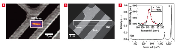 |
| a) Elastic scattering image of a CNT-FET taken without PMMA and top gold mirror. Inset: Raman scattering (G-band) intensity image of an isolated nanotube. b) Scanning electron micrograph of the same device. c) Raman spectrum measured for the same nanotube. Inset: Raman band associated with the radial breathing mode (RBM). (Reprinted with permission from Nature Publishing Group) |
| In recent work reported in Nature Nanotechnology ("A microcavity-controlled, electrically-driven, on-chip nanotube emitter at infrared wavelengths"), Xia and his colleagues at the Department of Nanometer Scale Science and Technology at IBM's Thomas J. Watson Research Center, led by Dr. Phaedon Avouris, have now realized cavity-controlled light emission from carbon nanotubes. |
| This is a first important step in the development of CNT-based, truly nanoscale light emitters. |
| The device demonstrated by the IBM team integrates a back-gated, light-emitting field effect transistor (FET) based on a single semiconducting single-walled CNT with a planar optical half-wavelength microcavity. |
| "Although the modification of emission properties of the light using optical cavities is well-known, the monolithic integration of a current-driven carbon nanotube light emitter and an optical cavity is challenging and has never been attempted" says Xia. |
| In their demonstration, Xia and his colleagues embedded the nanotube emitter in the middle of a planar optical cavity to maximize the interaction of the emitter dipole and the cavity field. They used low temperature atomic layer deposition (ALD) to enhance the overall quality of dielectric stacks which function as both optical cavity material and gate dielectric of the nanotube emitter. |
| Xia explains that the photonic microcavity consists of three dielectric layer stacks: 250 nm of polymethyl methacrylate (PMMA), 22 nm of ALD-deposited aluminum oxide, and 250 nm of silicon oxide sandwiched between a top gold mirror (20 nm) and a parallel bottom silver mirror (100 nm). An individual CNT is placed on top of the aluminum oxide layer close to the microcavity center and is orientated parallel to the silver and the gold mirrors to provide optimum coupling conditions between the nanotube and the available photonic microcavity modes. |
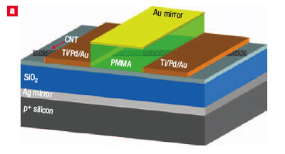 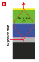 |
| Schematic view of the integrated device and its electronic properties. a) 3D schematic representation of the microcavity-controlled infrared nano-light source comprising an FET integrated with a planar half-wavelength (λ/2) microcavity. The source and drain electrodes made from Ti/Pd/Au (1/20/20 nm) are separated by 2 mm. b) Schematic λ/2 photonic mode profile showing the geometrical overlap of the nanotube and the spatial intensity distribution. The microcavity is formed by the Au and Ag mirrors and the light is emitted through the top Au mirror. The red arrow shows the emission direction of the on-axis mode. (Reprinted with permission from Nature Publishing Group) |
| Xia points out that integrating nanotube light emitters with high Q optical cavities (see more about the Q-factor in our Spotlight "Towards spooky nanotechnology with dynamic control of nanocavity Q") is one of the important research directions. "High performance, truly nanoscale light emitting devices (even nanolasers) can possibly be realized. The major challenge before realization of practical nanophotonic devices is our inability to produce multiple, identical (at least similar), and high quality nanotubes in desirable locations of the wafer. Actually this is a general problem in the development of nanotube based electronic and photonic devices. Some progresses have been made along this research directions recently." |
 By
Michael
Berger
– Michael is author of four books by the Royal Society of Chemistry:
Nano-Society: Pushing the Boundaries of Technology (2009),
Nanotechnology: The Future is Tiny (2016),
Nanoengineering: The Skills and Tools Making Technology Invisible (2019), and
Waste not! How Nanotechnologies Can Increase Efficiencies Throughout Society (2025)
Copyright ©
Nanowerk LLC
By
Michael
Berger
– Michael is author of four books by the Royal Society of Chemistry:
Nano-Society: Pushing the Boundaries of Technology (2009),
Nanotechnology: The Future is Tiny (2016),
Nanoengineering: The Skills and Tools Making Technology Invisible (2019), and
Waste not! How Nanotechnologies Can Increase Efficiencies Throughout Society (2025)
Copyright ©
Nanowerk LLC
|

Become a Spotlight guest author! Join our large and growing group of guest contributors. Have you just published a scientific paper or have other exciting developments to share with the nanotechnology community? Here is how to publish on nanowerk.com.
