| Posted: Oct 29, 2008 |
Boron nanowires shape up to be excellent field emission nanomaterials |
| (Nanowerk Spotlight) Nanostructured boron and boron-related compounds have attracted considerable scientific attention to exploit their potential use in high temperature electronics, thermoelectrics, and photovoltaics due to their unique chemical and physical properties, such as chemical inertness, hardness, and adjustable energy bandgap. Boron's theoretical tubular structures may even have higher electrical conductivity than carbon nanotubes (CNTs). |
| So far, carbon nanotubes have been considered the most promising material for field emitters, for instance as electron emitters for field emission displays (FED). Field emission results from the tunneling of electrons from a metal tip into vacuum, under application of a strong electric field. The small diameter and high aspect ratio of CNTs is very favorable for field emission. |
| Due to the still existing difficulties of synthesizing CNTs with uniform chirality, a number of technical questions – such as stability, low melting point and uniformity of field emission – remain to be overcome. That's why scientists are still looking to find other ideal candidates. New experiments conducted by scientists in China suggest that boron nanowires might fit the bill. |
| "So far, to our knowledge, while both amorphous and crystalline boron nanowires have been fabricated by magnetron sputtering, laser ablation, or chemical vapor methods, vertical arrays of single-crystal boron nanowires over a large area have not been synthesized in a one-step process" Dr. Hongjun Gao explains to Nanowerk. "In addition, little attention has been paid to the measurements of the physical properties of an individual boron nanowire." |
| Gao, a professor of physics and Director, Nanoscale Physics and Devices Laboratory at the Institute of Physics, Chinese Academy of Sciences, in Beijing, together with Prof. Ningsheng Xu and collaborators from the State Key Laboratory of Optoelectronic Materials and Technologies Guangdong Province Key Laboratory of Display Material and Technology at Sun Yat-sen University in Guangzhou, reports the successful synthesis of high-density, vertically aligned single-crystal boron nanowire arrays with a nanowire diameter of approximately 20–40nm by a thermal carbon-reduction method. The team published their findings in Advanced Materials ("Fabrication of Vertically Aligned Single-Crystalline Boron Nanowire Arrays and Investigation of Their Field-Emission Behavior"). |
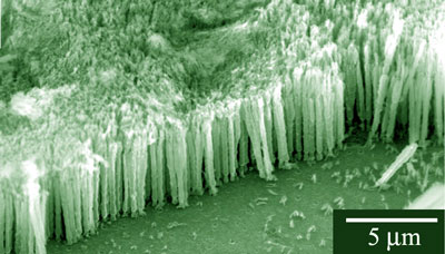 |
| Scanning electron microscopy images of large area aligned single crystal boron nanowire arrays. The as-prepared nanowires have uniform diameter and length, and stand vertically on the substrate. (Image: Dr. Gao, CAS) |
| Gao explains that the element boron is becoming more and more popular among the cold cathode candidates due to its particular structure and properties: "In a boron atom, the number of valence electrons is lower than that of available orbitals. Elements in this situation usually adopt metallic bonding, but the small size and high ionization energies of boron result in covalent rather than metallic bonding. So boron bonds through a unique 3-center 2-electron bond, making it possible to form a B12 icosahedron structural unit. This basic structure unit can form different boron structures (α-Rhombohedral, β-Rhombohedral and α-tetragonal) which result in different physical and chemical properties." |
| Theoretical analysis indicates that boron is able to form stable metallic nanotubes with properties superior to those of carbon nanotubes in field emission applications. Thus, one-dimensional boron nanostructures are viewed as having great potential – possibly greater than carbon nanotubes – in the development of field emitters, nanoelectronics, transducers, superconductors, and tips for scanning probe microscopes. |
| The Chinese scientists performed their experiments on individual boron nanowires and boron nanowire film, respectively. They developed a thermal carbon reduction method to synthesize high-density, vertically aligned single-crystal boron nanowire arrays with diameter of 20-40 nm. Boron powder and boron oxide powder are used as source materials, and the catalysts are magnetite nanoparticles. |
| "This is a new route for the growth of large area aligned boron nanowire arrays in one step, which is easier to control and more simple than other known methods" says Gao. "Moreover, we measured the field emission behavior of an individual boron nanowire, for the first time to our knowledge, and compared it with boron nanowire film – something that is very helpful for understanding the real field emission properties and the emission mechanism." |
| The experimental results obtained by Gao and his colleagues show that the boron nanowires are perfect single-crystals with a tetragonal structure and a growth direction along [001]. Measuring the conductivity, field emission, enhancement factor and emission stability of an individual boron nanowire, the team found that these values are comparable to the best results achieved with other nanomaterials that are considered to have excellent field emission properties. |
| "All these measurement results suggest that boron nanowire can be an excellent field emission material candidate" says Gao. "In addition, we showed that boron nanomaterial is not only an ideal cold cathode material in the field emission area but, because of its high melting point and emission stability, also has a potential application in high temperature semiconductor devices, field effect transistors or microwave devices." |
| Despite the fact that they appear to make a better cold-cathode material than most other candidates, there are some problems in applying boron nanowires in FEDs. Gao points out that the work function (i.e. the minimum energy required by a photon to remove an electron from the surface of a metal) of boron nanowires is not low enough, which results in a higher turn-on field than that required for CNT-based FEDs. Another is that the growth density of boron nanowires is not easy to control, which can influence the emission properties of thin film. |
| Lastly, according to Gao, the effect of the morphology, crystallinity, and contact conductance of the individual boron nanowires on their field emission properties is still under investigation because these measurements could provide more decisive interpretations on the field-emission mechanism. |
| "These three areas are the main thrust of our investigations and research" says Gao. "If all these questions can be resolved satisfactorily, we believe that boron nanowire will find use in practical applications in the not too distant future." |
 By
Michael
Berger
– Michael is author of four books by the Royal Society of Chemistry:
Nano-Society: Pushing the Boundaries of Technology (2009),
Nanotechnology: The Future is Tiny (2016),
Nanoengineering: The Skills and Tools Making Technology Invisible (2019), and
Waste not! How Nanotechnologies Can Increase Efficiencies Throughout Society (2025)
Copyright ©
Nanowerk LLC
By
Michael
Berger
– Michael is author of four books by the Royal Society of Chemistry:
Nano-Society: Pushing the Boundaries of Technology (2009),
Nanotechnology: The Future is Tiny (2016),
Nanoengineering: The Skills and Tools Making Technology Invisible (2019), and
Waste not! How Nanotechnologies Can Increase Efficiencies Throughout Society (2025)
Copyright ©
Nanowerk LLC
|

Become a Spotlight guest author! Join our large and growing group of guest contributors. Have you just published a scientific paper or have other exciting developments to share with the nanotechnology community? Here is how to publish on nanowerk.com.
