| Posted: Sep 14, 2006 |
Light sensors made from carbon nanotube macrobundles |
| (Nanowerk Spotlight) The photoconductivity of carbon nanotubes (CNTs) has been studied theoretically in a nanotube p-n junction, a single SWNT transistor, and thin SWNT films. While individual nanotubes generate discrete fine peaks in optical absorption and emission, macroscopic structures consisting of many CNTs gathered together also demonstrate interesting optical behavior. |
| For example, a millimeter-long bundle of aligned multi-walled nanotubes (MWNTs) emits polarized incandescent light by electrical current heating, and recently researchers in China have made multi-walled nanotubes (SWNT) bundles giving higher brightness emission at lower voltage compared with conventional tungsten filaments. |
| Recent achievements in fabricating self-assembled centimeter-long bundles of CNTs have greatly facilitated study on the macroscopic behavior of these bundle structures. Preliminary results such as an optical polarizer and a light bulb based on CNT macrobundles have been reported. |
| Researchers at Tsinghua University in Beijing/PR China now have constructed a simple setup with macrobundles, up to 50 µm wide, consisting of thousands of aligned CNTs suspended between two electrodes, which can sense the incident visible and infrared light through the difference of current flowthrough the bundle. |
| Dr. Jinquan Wei from the Department of Mechanical Engineering, Key Lab for AMMPT of Education Ministry, at Tsinghua University, first author of a recent paper describing theses findings, explained the research to Nanowerk: "Several types of nanotubes (SWNTs, DWNTs, and MWNTs) were tested and each of them shows distinct response upon light illumination in terms of the magnitude and direction of current difference. We calculated important parameters for photosensors, such as response time and energy efficiency. Such results demonstrate that nanotube macrostructures are promising candidates for constructing infrared/visible sensors." |
| The paper, titled "Carbon Nanotube Macrobundles for Light Sensing", appeared in the July 28, 2006 online edition of Small. |
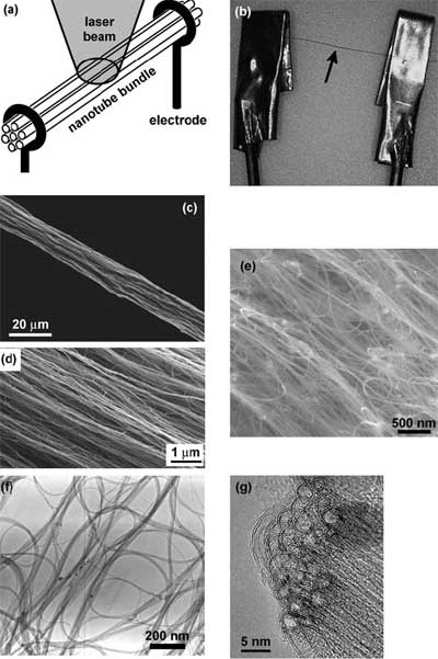 |
| Experimental setup and characterization of nanotube bundles: a) Illustration of the setup containing a nanotube bundle suspended between two electrodes and illuminated by a laser beam at the middle portion. b) Photo of a nanotube bundle (see arrow) clamped by two copper sticks through nickel foils. c) Low-magnification SEM image of a nanotube bundle with a width of 20 mm. d) Higher magnification SEM image of aligned nanotubes in a MWNT bundle. e) SEM image of a DWNT bundle showing different morphology to the MWNTs. f) TEM image of as-grown DWNTs displaying very low levels of (catalyst) particles in the sample. g) High-resolution TEM image along the edge of a DWNT bundle revealing its double-walled tube structure. (Reprinted with permission from Wiley-VCH Verlag) |
| "Before our experiments, while the photoconductivity of CNTs has been studied theoretically, a significant current change in CNTs has never been observed experimentally" says Wei. "More importantly, we observed that the photocurrent behaviors of SWNTs and DWNTs are quite different from those of MWNTs." |
| In contrast to SWNTs and DWNTs, current flow in the MWNT bundle slightly increased upon laser illumination and the response time of SWNTs upon laser turn on/off is much faster than MWNTs. The intrinsic electronic structure of nanotubes is believed to be a factor contributing to the different direction of current change. |
| "One disappointment here is the relatively low energy-conversion efficiency (<1%) observed in the CNT bundles" says Wei. "We expect an improvement in efficiency in our future work through synthesizing clean, all semiconducting nanotubes, or making smaller and flattened bundles." |
| "Bottomline, however, is that our research not only provides some exciting experimental results, but also shows that CNTs can be used in nanoscale optoelectronic and photonic applications." |
 By
Michael
Berger
– Michael is author of four books by the Royal Society of Chemistry:
Nano-Society: Pushing the Boundaries of Technology (2009),
Nanotechnology: The Future is Tiny (2016),
Nanoengineering: The Skills and Tools Making Technology Invisible (2019), and
Waste not! How Nanotechnologies Can Increase Efficiencies Throughout Society (2025)
Copyright ©
Nanowerk LLC
By
Michael
Berger
– Michael is author of four books by the Royal Society of Chemistry:
Nano-Society: Pushing the Boundaries of Technology (2009),
Nanotechnology: The Future is Tiny (2016),
Nanoengineering: The Skills and Tools Making Technology Invisible (2019), and
Waste not! How Nanotechnologies Can Increase Efficiencies Throughout Society (2025)
Copyright ©
Nanowerk LLC
|

Become a Spotlight guest author! Join our large and growing group of guest contributors. Have you just published a scientific paper or have other exciting developments to share with the nanotechnology community? Here is how to publish on nanowerk.com.
