| Posted: Sep 27, 2006 |
Flipping the spin... |
| (Nanowerk Spotlight) Spintronics (short for "spin-based electronics") is an emergent technology which exploits the quantum propensity of electrons to spin as well as making use of their charge state. The spin itself is manifested as a detectable weak magnetic energy state characterized as "spin up" and "spin down". Spin flip length is an important parameter to know for designing spintronics devices. Because in spintronics, electron spin carries the information, it is important to know how far electrons can travel in a device before this spin information is lost. In a discovery that could contribute to the emerging field of spintronics, scientists at Oak Ridge National Laboratory (ORNL) and the Institute of Physics, Chinese Academy of Science, have demonstrated a way to measure the distance an electron travels in nanoscale materials before its spin is reversed due to scattering. |
| Such measurements are difficult to achieve outright because electrons' spins in a nonmagnetic material rarely flip until they travel a distance many times the size of the device itself. This means that possibly just a small fraction of electrons flip inside a nanoscale device, an attribute that may make electrons' magnetic properties attractive for storage, sensors and, potentially, quantum computing. |
| Because of the very long spin-flip length (hundreds of nanometers), reliable determination of the strength of spin-flip scattering in the past required the use of metal wires many times the length of the mean-free-path. ORNL theoretical physicist Xiaoguang Zhang, from the Center for Nanophase Materials Sciences at ORNL used data provided by Chinese colleagues to determine that the measurement could be made by comparing the magnetoresistance of electrons traveling through single and double layer arrangements of an insulating material. |
| Zhang explains the recent findings to Nanowerk: "In magnetic multilayers and tunnel junctions the size of the constituent layers rarely reaches the diffusive regime. Most of these layers are nanometers in thickness and electron transport in these layers are nearly ballistic. So far there has not been an experimental approach that allows the study of spin-flip scattering near the ballistic limit. A further motivation for studying spin-flip scattering in nanometer sized films is the effect of a large bias. While the voltage effect over a long metal wire is almost certainly linear, there can be large nonlinear effects of the same voltage over a one-nanometer thin film." |
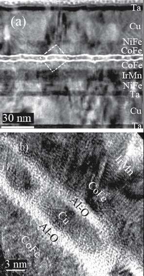 |
| A cross-sectional TEM image of a typical double barrier magnetic tunnel junction with copper (Cu) spacer. (a) is low-magnification image and (b) is the corresponding HRTEM images. The actual Cu thickness is much larger than the nominal thickness of 1.4 nm. (Reprinted with permission from The American Physical Society) |
| In a recent paper in Physical Review Letters ("Probing Spin-Flip Scattering in Ballistic Nanosystems"), Zhang and his collaborators present a novel experimental approach to the study of spin-flip scattering in ultrathin metal films in the ballistic regime. |
| "The key to our new approach is to reduce the channel conductance for each spin to the same order as the spin-flip conductance between the two spin channels, without reducing the electron mean-free-path or increasing the sample size" says Zhang. "Tunnel barriers are the obvious choice to serve this purpose. By sandwiching a thin copper film between two tunnel barriers, the voltage and temperature dependence of the spin-flip conductance between the two spin channels in the copper layer can be extracted from the tunneling magnetoresistance (TMR) measurements." |
| The researchers found that the spin-flip scattering increases linearly with the temperature and at a rate proportional to the copper layer thickness. This argues for a phononic origin of spin-flip scattering. |
 By
Michael
Berger
– Michael is author of four books by the Royal Society of Chemistry:
Nano-Society: Pushing the Boundaries of Technology (2009),
Nanotechnology: The Future is Tiny (2016),
Nanoengineering: The Skills and Tools Making Technology Invisible (2019), and
Waste not! How Nanotechnologies Can Increase Efficiencies Throughout Society (2025)
Copyright ©
Nanowerk LLC
By
Michael
Berger
– Michael is author of four books by the Royal Society of Chemistry:
Nano-Society: Pushing the Boundaries of Technology (2009),
Nanotechnology: The Future is Tiny (2016),
Nanoengineering: The Skills and Tools Making Technology Invisible (2019), and
Waste not! How Nanotechnologies Can Increase Efficiencies Throughout Society (2025)
Copyright ©
Nanowerk LLC
|

Become a Spotlight guest author! Join our large and growing group of guest contributors. Have you just published a scientific paper or have other exciting developments to share with the nanotechnology community? Here is how to publish on nanowerk.com.
