| Posted: Oct 12, 2006 |
Essential characteristics of self-assembled quantum dots |
| (Nanowerk Spotlight) Semiconductor photonics, electronics and optoelectronics infrastructure is at the core of the information society. As the length scales of electronic devices continue to shrink, the cost of traditional approaches to device fabrication involving lithography is becoming excessive. It is regarded that self-assembled growth methods are a solution to the problem of fabricating smaller devices at a lower cost. Self-assembled quantum dots (QDs) are providing the possibility of new devices for this infrastructure in the short, medium and long term. QDs are ideal for the study of the fundamental properties of nanostructures, which is applicable across the nanotechnology and nanoscience sector. Research in self-assembled semiconductor QDs is therefore characterized by a remarkably well-matched combination of the two main motivations for scientific research, namely academic interest and the potential for industrial applications. As a consequence, there is an intense scientific activity in materials growth, structural characterization, optical and transport spectroscopy, device engineering and computational modeling. The field of self-assembled semiconductor nanostructures started in 1985 in Europe by a French group at the Centre National d'Etudes des Telecommunications - CNET ("Growth by molecular beam epitaxy and characterization of InAs/GaAs strained-layer superlattices"). |
| Self-assembled QDs are spontaneously formed when a few monolayers of a semiconductor material are deposited on a substrate with a lattice mismatch of about 5%. Semiconductor heterostructures containing self-assembled QDs are of fundamental interest because they provide a relatively simple means of producing an array of quantum potentials in which electrons and holes are confined in discrete quasi-atomic (or zero-dimensional) energy states. By varying the materials involved, the growth conditions, and by vertically stacking layers of nanostructures, a rich variety of novel materials can be produced for the study of the fundamental properties of strongly confined systems, and for the development of advanced electronic and photonic devices and quantum-functional and memory devices. |
| Dr. Mohamed Henini from the School of Physics & Astronomy ast the University of Nottingham in the UK explained the potential of self-assembled QDs to Nanowerk: "Among the devices that could benefit from the self-assembled QDs are volatile and non-volatile semiconductor memory and hard disk materials. Light emitters and detectors incorporating a single self-organized quantum dot as the active element, are arguably the most viable approaches to practical single photon generation and detection. These devices could be used in quantum cryptography, regarded by many as the ultimate solution for secure network communications, which would alleviate concerns surrounding present day software based techniques. In the longer term, quantum information systems, for example for secure transmission, promise to revolutionize the way in which we communicate, store and process information." |
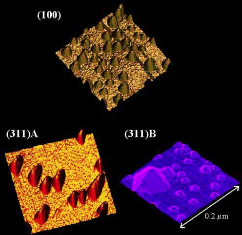 |
| Scanning tunnelling microscope pictures (200 x 200 nm) of InAs/GaAs QDs grown by MBE on (100), (311)A and (311)B GaAs substrates. As can be seen, using substrates with different orientation can control the shape of the QDs. (Reprinted with permission from Springer) |
| Several methods for the fabrication of QDs have been reported over the last decade including lithography-based technologies. Although this technique is widely used to provide QD predominantly by the combination of high-resolution electron beam lithography and etching, the spatial resolution required for reaching the size regime where significant quantization effects can be expected tends to be larger than the desirable level. In addition, lithographic methods and subsequent processing often produce contamination, defect formation, size non-uniformity, poor interface quality, and even damage to the bulk of the crystal itself. A new attractive method of defect free 10 nm scale QD fabrication is the Stranski?Krastanov (SK) growth in lattice-mismatched systems. The advantages of this technique of QD fabrication are that no nanotechnology and no further etch or implantation induced process is necessary. Since the dots are grown in-situ a homogeneous surface morphology is maintained and defect creation is avoided. However, the inherent problem associated with this method is the size non-uniformity and the position uncontrollability of the QD. Controlling the dimension and arrangement of the self-organized 3D structures is thought to be very important for obtaining good properties of the structures. |
| Many challenges remain in the development of high-performance QD devices. Dr. Henini points out three examples: |
| Lasers |
| Semiconductor lasers have opened up potentially huge markets in optical communication, compact disks and related optical data storage applications, displays and lighting. Long distance signal transmission over optical fiber require two wavelength windows, namely 1300 nm and 1550 nm, at which absorption effects are minimized. Considerations for a commercially viable diode are that that the QD-based lasers need to be improved in order to achieve high output power and long lifetime. |
| Quantum Dot Infrared Photodetectors |
| "All important applications of infrared techniques, both for military and civil purposes (sciences, meteorology, medicine, industry, etc) rely on the detection of radiation in the 1-3 µm, 3-5 µm and 8-14 µm spectral range (the so-called atmospheric windows). The 8-14 µm wavelength region is especially important for imaging since the temperature of the human and environments bodies is around 300°K corresponding to a peak wavelength of thermal radiation of about 10 µm." (Source) |
| The materials, which cover the above wavelength regions, include II-VI, III-V and IV-VI compound semiconductors. With respect to the well-known HgCdTe detectors, GaAs/AlGaAs quantum wells devices have a number of potential advantages including the use of standard manufacturing technology based on advanced GaAs growth and processing techniques, highly uniform and well controlled MBE growth on large GaAs wafers, high yield, greater thermal stability, and intrinsic radiation hardness. |
| Recently, there has been significant interest in developing novel QD infrared photodetectors (QDIPs). "There are two major potential advantages of quantum dots over quantum wells as photodetectors, namely: (1) intersubband absorption may be allowed at normal incidence. In quantum well infrared photodetectors (QWIPs) only transitions polarized perpendicular to the growth direction are allowed, due to absorption selection rules. The selection rules in QDIPs are inherently different, and normal incidence absorption is, indeed, observed, (2) thermal generation of electrons is significantly reduced due to the energy quantization in all three dimensions. Generation by LO phonons is prohibited unless the gap between the discrete energy levels equals exactly to that of the phonon. This prohibition does not apply to quantum wells, since the levels are quantized only in the growth direction and a continuum exists in the other two. Hence thermal-generation or recombination by LO phonons results, with a capture time of few picoseconds. Thus, it is expected that the signal-to-noise ratio in QDIPs will be significantly larger than that of QWIPs." (Source) |
| Optical data storage |
| "Another application is an optical data storage medium, in which bits of information are stored as a single or few electrons within the dots. These memory devices based on QDs should require a very low switching energy because the information is stored as a single or few electrons. Optical illumination can be used to write the charge to be stored in the QDs. It is predicted that because each QD would carry a bit of information, the memory devices could potentially achieve ultra dense storage capacities of Terabit/in." (Source) |
| Some of the studies reported in international journals are still in their infancy and many challenges remain in the development of these devices. |
| SANDiE Network of Excellence |
| The future directions in the field of self-assembled nanostructures (SAN) is witnessed by the newly funded (9.2 million Euro, 48 months from autumn 2004) EU Framework 6 Network of Excellence Project "Self-Assembled semiconductor Nanostructures for new Devices in photonics and Electronics" (SANDiE). This network, which will carry out research into self-assembled semiconductor nanostructures, involves 28 leading academic and industrial research laboratories in eleven countries. |
| The scientific goals of the Network will lead to advances in Information Technology, for example by faster, better and completely novel devices for the telecommunications industry. Also advances in sustainability are made by using SAN for devices with lesser energy consumption. In addition, SAN offer advantages in hard radiation environment, contributing to space applications. |
| Dr. Henini recently published a paper, titled "Properties and applications of quantum dot heterostructures grown by molecular beam epitaxy" that appeared in the July 26, 2006 edition of the free-access Nanoscale Research Letters. |
 By
Michael
Berger
– Michael is author of four books by the Royal Society of Chemistry:
Nano-Society: Pushing the Boundaries of Technology (2009),
Nanotechnology: The Future is Tiny (2016),
Nanoengineering: The Skills and Tools Making Technology Invisible (2019), and
Waste not! How Nanotechnologies Can Increase Efficiencies Throughout Society (2025)
Copyright ©
Nanowerk LLC
By
Michael
Berger
– Michael is author of four books by the Royal Society of Chemistry:
Nano-Society: Pushing the Boundaries of Technology (2009),
Nanotechnology: The Future is Tiny (2016),
Nanoengineering: The Skills and Tools Making Technology Invisible (2019), and
Waste not! How Nanotechnologies Can Increase Efficiencies Throughout Society (2025)
Copyright ©
Nanowerk LLC
|

Become a Spotlight guest author! Join our large and growing group of guest contributors. Have you just published a scientific paper or have other exciting developments to share with the nanotechnology community? Here is how to publish on nanowerk.com.
