| Posted: Feb 09, 2009 |
Nanotechnology heaters and thermometers for thermal processing of nanomaterials |
| (Nanowerk Spotlight) Nearly every chemical or physical property of materials depends upon temperature, and researchers are only beginning to understand the huge breadth of applications that nanoscale heaters could facilitate. For example, scientists have previously demonstrated that a micro-heater built into an atomic force microscope can be used instead of a large furnace that is normally used to grow nanotubes as part of the chemical vapor deposition process. The tiny device provided highly-localized heating for only the locations where researchers wanted to grow the nanostructures. |
| While most previous research on this kind of microcantilever heaters and thermometers used device elements that were several micrometers in size, researchers have now reported an approach to fabricate a 100 nanometer-sized heater/thermometer using contact photolithography and controlled anneal conditions. A deep understanding of nanomaterials requires nanoscale probes (also see our previous Nanotechnology Spotlight: How to build a nanothermometer). With such nanoscale heater/thermometer devices it becomes possible to test the temperature dependence of materials properties at the very smallest scale and perform thermal diagnostics of nanomaterials. |
| "We have developed a simple batch fabrication process to form a 100 nm scale heater/thermometer on a silicon cantilever, both with a tip and in the absence of a tip," William P. King tells Nanowerk. "The heater is first fabricated onto a cantilever having no tip, and then integrated into a sharp tip. These heated cantilevers can be batch fabricated at reasonably low cost." |
| King, an associate professor and Kritzer Faculty Scholar in the Mechanical Engineering Laboratory at the University of Illinois at Urbana-Champaign, explains that the nanoscale heater can efficiently direct tiny quantities of heat with nanoscale resolution. |
| The results of this work, for which King collaborated with scientists from the Department of Mechanical Engineering and Applied Mechanics at the University of Rhode Island, has been published in the February 6, 2009 online edition of Nanotechnology (A 100 nanometer scale resistive heater–thermometer on a silicon cantilever). |
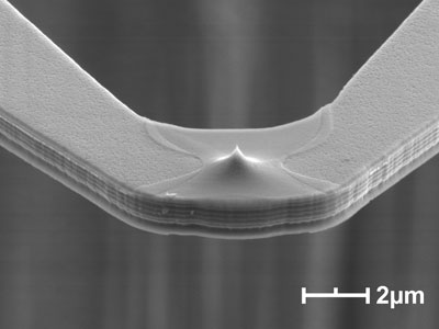 |
| Scanning electron microscope images of a nanoheater cantilever with a sharp tip. The heater is located at the end of cantilever structure and the cantilever is 1.5 µm thick. The tip is in the middle of two highly doped areas. (Image: Dr. King, University of Illinois at Urbana-Champaign) |
| King explains that in order to form a heater/thermometer at the end of a silicon cantilever, the photolithographically defined highly doped regions are first implanted with boron, and then a high temperature annealing process causes the dopants to laterally diffuse in a way that shrinks the heater region to about 100 nm. |
| "When the silicon is annealed at high temperature, the dopants diffuse within the silicon, narrowing the gap," says King. "Careful control of the annealing conditions allows the major carriers at the middle point between two high doping areas to change from N type to P type and the dopant concentration to reach 1017 atoms per cubic centimeter. Under these conditions, the resulting nanoheater will be as small as 100 nm. The reason we chose this counter doping scheme is to restrict the electrical current to only flow through the nanoheater region." |
| The basic fabrication process that the team used is very similar to the fabrication process for silicon AFM cantilevers having integrated heaters, with the exception that the goal here was to fabricate a tipless cantilever with a 100 nm heater/thermometer. |
| King says that, having achieved a 100 nm scale resistive heater/thermometer in a silicon cantilever, the next challenge was to integrate this heater onto a tip at the free end of a silicon cantilever. This fabrication process starts with making sharp tips on a silicon on insulator wafer and the tips are made with a standard oxide sharpening process. After the sharp tips are made, the cantilever structures are defined by photolithography followed by dry etch in inductively coupled plasma. |
| By applying a voltage pulse to the cantilever, the temperature of the nanoheater at the tip increases to steady state under sufficient pulse duration. When the pulse is stopped, the cantilever temperature drops to its initial value. |
| King points out that the thermal conductance within and from the cantilever is important for thermal sensing. "While the focus of this particular work has been on heating and not temperature sensing, it is possible to comment on how the thermal conductance from the nanoheater compares to larger heaters. There are also important differences in thermal conductance for the case of the cantilever freely suspended in air compared to a cantilever operated close to a substrate" |
| s Since these heated cantilevers can be batch fabricated in a low-cost process they hold great promise for use in a wide range of applications. King says that his team is already working on many applications of heated cantilever tips for nanoscale thermal processing, including nanoscale manufacturing, metrology, and materials analysis. |
 By
Michael
Berger
– Michael is author of four books by the Royal Society of Chemistry:
Nano-Society: Pushing the Boundaries of Technology (2009),
Nanotechnology: The Future is Tiny (2016),
Nanoengineering: The Skills and Tools Making Technology Invisible (2019), and
Waste not! How Nanotechnologies Can Increase Efficiencies Throughout Society (2025)
Copyright ©
Nanowerk LLC
By
Michael
Berger
– Michael is author of four books by the Royal Society of Chemistry:
Nano-Society: Pushing the Boundaries of Technology (2009),
Nanotechnology: The Future is Tiny (2016),
Nanoengineering: The Skills and Tools Making Technology Invisible (2019), and
Waste not! How Nanotechnologies Can Increase Efficiencies Throughout Society (2025)
Copyright ©
Nanowerk LLC
|

Become a Spotlight guest author! Join our large and growing group of guest contributors. Have you just published a scientific paper or have other exciting developments to share with the nanotechnology community? Here is how to publish on nanowerk.com. |
